CYRF89435
®
PRoC™ - CapSense
PRoC™ - CapSense®
❐
■
Single Device, Two functions
❐ 8-bit flash based CapSense controller MCU function and
2.4-GHz WirelessUSB™ NL radio transceiver function in a
single device
■
Wide operating range: 1.9 V to 3.6 V
❐ Configurable capacitive sensing elements
❐ 7 ȝA per sensor at 500 ms scan rate
❐ Supports SmartSense™ Auto-tuning
®
❐ Supports a combination of CapSense buttons, sliders, and
proximity sensors
❐ SmartSense_EMC offers superior noise immunity for
applications with challenging conducted and radiated noise
conditions
■
RF Attributes
❐ 2.4-GHz WirelessUSB-NL Transceiver function
❐ Operates in the 2.4-GHz ISM Band (2.402 GHz - 2.479 GHz)
❐ 1-Mbps over-the-air data rate
❐ Receive sensitivity typical: –87 dBm
❐ 1 ȝA typical current consumption in sleep state
❐ Closed-loop frequency synthesis
❐ Supports frequency-hopping spread spectrum
❐ On-chip packet framer with 64-byte first in first out (FIFO)
data buffer
❐ Built-in auto-retry-acknowledge protocol simplifies usage
❐ Built-in cyclic redundancy check (CRC), forward error
correction (FEC), data whitening
❐ Additional outputs for interrupt request (IRQ) generation
❐ Digital readout of received signal strength indication (RSSI)
■
MCU Attributes
❐ Powerful Harvard-architecture processor
❐ M8C CPU – Up to 4 MIPS with 24 MHz Internal clock, external
crystal resonator or clock signal
❐ Low power at high speed
■
Temperature range: 0 °C to +70 °C
■
Flexible on-chip memory
• 32 KB Flash/2 KB SRAM
❐ 50,000 flash erase/write cycles
❐ Partial flash updates
❐ Flexible protection modes
Cypress Semiconductor Corporation
Document Number: 001-76581 Rev. *G
•
In-system serial programming (ISSP)
■
Precision, programmable clocking
❐ Internal main oscillator (IMO): 6/12/24 MHz ± 5%
❐ Internal low-speed oscillator (ILO) at 32 kHz for watchdog
and sleep timers
❐ Precision 32 kHz oscillator for optional external crystal
■
Programmable pin configurations
❐ Up to 13 general-purpose I/Os (GPIOs)
❐ Dual mode GPIO: All GPIOs support digital I/O and analog
inputs
❐ 25-mA sink current on each GPIO
• 120 mA total sink current on all GPIOs
❐ Pull-up, high Z, open-drain modes on all GPIOs
❐ CMOS drive mode –5 mA source current on ports 0 and 1
and 1 mA on port 2
❐ 20 mA total source current on all GPIOs
■
Versatile analog system
❐ Low-dropout voltage regulator for all analog resources
❐ Common internal analog bus enabling capacitive sensing on
all pins
❐ High power supply rejection ratio (PSRR) comparator
❐ 8 to 10-bit incremental analog-to-digital converter (ADC)
■
Additional system resources
2
❐ I C slave:
• Selectable to 50 kHz, 100 kHz, or 400 kHz
❐ SPI master and slave: Configurable 46.9 kHz to 12 MHz
❐ Three 16-bit timers
❐ Watchdog and sleep timers
❐ Integrated supervisory circuit
❐ Emulated E2PROM using flash memory
■
Complete development tools
❐ Free development tool (PSoC Designer™)
❐ Full-featured, in-circuit emulator (ICE) and programmer
❐ Full-speed emulation
❐ Complex breakpoint structure
❐ 128 KB trace memory
■
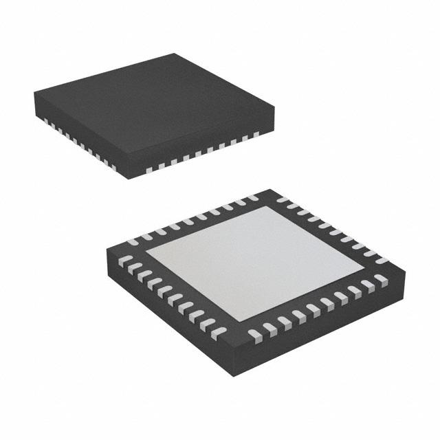
Package option
❐ 40-pin 6 mm × 6 mm QFN
198 Champion Court
•
San Jose, CA 95134-1709
•
408-943-2600
Revised May 18, 2017
Not recommended for new designs
PRoC-CS Features
�CYRF89435
Logical Block Diagram
Port 2
Port 1
Port 0
PWR Sys
(Regulator)
Prog. LDO
System Bus
PSoC Core
SRAM
2048 Bytes
32K Flash
SROM
Sleep and
Watchdog
CPU Core (M8C)
Interrupt
Controller
Not recommended for new designs
Global Analog Connect
Internal Low Speed Oscillator (ILO
6/12/24 MHz Internal Main Oscillator
Multiple Clock Sources
Analog
Reference
CapSense
System
CapSense
CapS
Module
Two
Comparators
Analog Mux
VOUT
VIN
WIRELESSUSB-NL
SYSTEM
VDD_IO
LDO Linear
Regulator
GFSK
Modulator
PKT
FIFO
RST_n
Framer
SPI Registers
PA
Synthesizer
ANT
ANTb
VCO
Pwr/ Reset
BRCLK
Xtal Osc
GFSK
Demodulator
X
Image
Rej . Mxr.
XTALi
I2C Slave
LNA + BPF
XTALo
Internal Voltage
References
System
Resets
SPI
Master/
Slave
Three 16 bit
Timers
POR
and
LVD
Digital
Clocks
SYSTEM RESOURCES
Document Number: 001-76581 Rev. *G
Page 2 of 39
�CYRF89435
PSoC® Functional Overview ............................................ 4
PSoC Core .................................................................. 4
CapSense System ....................................................... 4
WirelessUSB-NL System ............................................ 5
Transmit Power Control ............................................... 5
Power-on and Register Initialization Sequence ........... 5
Getting Started .................................................................. 6
CapSense Design Guides ........................................... 6
CYPros Consultants .................................................... 6
Solutions Library .......................................................... 6
Technical Support ....................................................... 6
Development Tools .......................................................... 7
PSoC Designer Software Subsystems ........................ 7
Designing with PSoC Designer ....................................... 8
Select User Modules ................................................... 8
Configure User Modules .............................................. 8
Organize and Connect ................................................ 8
Generate, Verify, and Debug ....................................... 8
Pinouts .............................................................................. 9
Pin Definitions ................................................................ 10
Electrical Specifications – PSoC Core ......................... 11
Absolute Maximum Ratings ....................................... 11
Operating Temperature ............................................. 11
DC Chip-Level Specifications .................................... 12
DC GPIO Specifications ............................................ 13
Analog DC Mux Bus Specifications ........................... 14
DC Low Power Comparator Specifications ............... 14
Comparator User Module Electrical Specifications ... 15
ADC Electrical Specifications .................................... 16
DC POR and LVD Specifications .............................. 17
DC Programming Specifications ............................... 17
DC I2C Specifications ............................................... 18
DC Reference Buffer Specifications .......................... 18
DC IDAC Specifications ............................................ 18
AC Chip-Level Specifications .................................... 19
Document Number: 001-76581 Rev. *G
AC GPIO Specifications ............................................ 20
AC Comparator Specifications .................................. 21
AC External Clock Specifications .............................. 21
AC Programming Specifications ................................ 22
AC I2C Specifications ................................................ 23
SPI Master AC Specifications ................................... 24
SPI Slave AC Specifications ..................................... 25
Electrical Specifications – RF Section ......................... 27
Initialization Timing Requirements ............................ 30
SPI Timing Requirements ......................................... 31
Packaging Information ................................................... 32
Thermal Impedances ................................................. 33
Capacitance on Crystal Pins ..................................... 33
Solder Reflow Specifications ..................................... 33
Development Tool Selection ......................................... 34
Software .................................................................... 34
Development Kits ...................................................... 34
Device Programmers ................................................. 34
Ordering Information ...................................................... 35
Ordering Code Definitions ......................................... 35
Acronyms ........................................................................ 36
Reference Documents .................................................... 36
Document Conventions ................................................. 36
Units of Measure ....................................................... 36
Numeric Naming ........................................................ 37
Glossary .......................................................................... 37
Document History Page ................................................. 38
Sales, Solutions, and Legal Information ...................... 39
Worldwide Sales and Design Support ....................... 39
Products .................................................................... 39
PSoC® Solutions ...................................................... 39
Cypress Developer Community ................................. 39
Technical Support ..................................................... 39
Page 3 of 39
Not recommended for new designs
Contents
�CYRF89435
The PSoC family consists of on-chip controller devices, which
are designed to replace multiple traditional microcontroller unit
(MCU)-based components with one, low cost single-chip
programmable component. A PSoC device includes
configurable analog and digital blocks, and programmable
interconnect. This architecture allows the user to create
customized peripheral configurations, to match the requirements
of each individual application. Additionally, a fast CPU, flash
program memory, SRAM data memory, and configurable I/O are
included in a range of convenient pinouts.
The architecture for this device family, as shown in the Logical
Block Diagram on page 2, consists of three main areas:
■
The Core
■
CapSense Analog System
■
WirelessUSB-NL System
■
System Resources.
A common, versatile bus allows connection between I/O and the
analog system.
from prototyping to mass production without re-tuning for
manufacturing variations in PCB and/or overlay material
properties.
SmartSense_EMC
In addition to the SmartSense auto-tuning algorithm to remove
manual tuning of CapSense applications, SmartSense_EMC
user module incorporates a unique algorithm to improve
robustness of capacitive sensing algorithm/circuit against high
frequency conducted and radiated noise. Every electronic device
must comply with specific limits for radiated and conducted
external noise and these limits are specified by regulatory bodies
(for example, FCC, CE, U/L and so on). A very good PCB layout
design, power supply design and system design is a mandatory
for a product to pass the conducted and radiated noise tests. An
ideal PCB layout, power supply design or system design is not
often possible because of cost and form factor limitations of the
product. SmartSense_EMC with superior noise immunity is well
suited and handy for such applications to pass radiated and
conducted noise test.
Figure 1. CapSense System Block Diagram
CS1
Each CYRF89435 device includes a dedicated CapSense block
that provides sensing and scanning control circuitry for
capacitive sensing applications. The 13 GPIOs provide access
to the MCU and analog mux.
IDAC
Analog Global Bus
PSoC Core
The PSoC Core is a powerful engine that supports a rich
instruction set. It encompasses SRAM for data storage, an
interrupt controller, sleep and watchdog timers, and IMO and
ILO. The CPU core, called the M8C, is a powerful processor with
speeds up to 24 MHz. The M8C is a 4-MIPS, 8-bit
Harvard-architecture microprocessor.
Reference
Buffer
Document Number: 001-76581 Rev. *G
Cinternal
Comparator
The analog system contains the capacitive sensing hardware.
Several hardware algorithms are supported. This hardware
performs capacitive sensing and scanning without requiring
external components. The analog system is composed of the
CapSense PSoC block and an internal 1 V or 1.2 V analog
reference, which together support capacitive sensing of up to
13 inputs. Capacitive sensing is configurable on each GPIO pin.
Scanning of enabled CapSense pins are completed quickly and
easily across multiple ports.
SmartSense is an innovative solution from Cypress that removes
manual tuning of CapSense applications. This solution is easy to
use and provides a robust noise immunity. It is the only
auto-tuning solution that establishes, monitors, and maintains all
required tuning parameters. SmartSense allows engineers to go
CSN
Vr
CapSense System
SmartSense
CS2
Cexternal (P0[1]
or P0[3])
Mux
Mux
Refs
Cap Sense Counters
CSCLK
IMO
CapSense
Clock Select
Oscillator
Page 4 of 39
Not recommended for new designs
PSoC® Functional Overview
�CYRF89435
The Analog Mux Bus can connect to every GPIO pin. Pins are
connected to the bus individually or in any combination. The bus
also connects to the analog system for analysis with the
CapSense block comparator.
Switch control logic enables selected pins to precharge
continuously under hardware control. This enables capacitive
measurement for applications such as touch sensing. Other
multiplexer applications include:
■
Complex capacitive sensing interfaces, such as sliders and
touchpads.
■
Chip-wide mux that allows analog input from any I/O pin.
■
Crosspoint connection between any I/O pin combinations.
On-chip transmit and receive FIFO registers are available to
buffer the data transfer with MCU. Over-the-air data rate is
always 1 Mbps even when connected to a slow, low-cost MCU.
Built-in CRC, FEC, data whitening, and automatic
retry/acknowledge are all available to simplify and optimize
performance for individual applications.
For more details on the radio’s implementation details and timing
requriements, please go through the WirelessUSB-NL datasheet
in www.cypress.com.
Figure 2. WirelessUSB-NL logic Block Diagram
VDD1 ...VDD7
VOUT
VIN
VDD_IO
LDO Linear
Regulator
GFSK
Modulator
PKT
Among the advantages of WirelessUSB-NL are its fast lock times
and channel switching, along with the ability to transmit larger
payloads. Use of longer payload packets, compared to multiple
short payload packets, can reduce overhead, improve overall
power efficiency, and help alleviate spectrum crowding.
Combined with Cypress's Capacitive touch sense controllers,
WirelessUSB-NL also provides the lowest bill of materials (BOM)
cost solution for sophisticated PC peripheral applications such
as wireless keyboards and mice, as well as best-in-class
wireless performance in other demanding applications. such as
toys, remote controls, fitness, automation, presenter tools, and
gaming.
With PRoC-CS, the WirelessUSB-NL transceiver can add
wireless capability to a wide variety of CapSense applications.
The WirelessUSB-NL is a fully-integrated CMOS RF transceiver,
GFSK data modem, and packet framer, optimized for use in the
2.4-GHz ISM band. It contains transmit, receive, RF synthesizer,
and digital modem functions, with few external components. The
transmitter supports digital power control. The receiver uses
extensive digital processing for excellent overall performance,
even in the presence of interference and transmitter
impairments.
The product transmits GFSK data at approximately 0-dBm
output power. Sigma-Delta PLL delivers high-quality DC-coupled
transmit data path.
The low-IF receiver architecture produces good selectivity and
image rejection, with typical sensitivity of –87 dBm or better on
most channels. Sensitivity on channels that are integer multiples
of the crystal reference oscillator frequency (12 MHz) may show
approximately 5 dB degradation. Digital RSSI values are
available to monitor channel quality.
Document Number: 001-76581 Rev. *G
CLK
MISO
MOSI
RST_n
PA
Framer
WirelessUSB-NL, optimized to operate in the 2.4-GHz ISM band,
is Cypress's third generation of 2.4-GHz low-power RF
technology. WirelessUSB-NL implements a Gaussian
frequency-shift keying (GFSK) radio using a differentiated
single-mixer, closed-loop modulation design that optimizes
power efficiency and interference immunity. Closed-loop
modulation effectively eliminates the problem of frequency drift,
enabling WirelessUSB-NL to transmit up to 255-byte payloads
without repeatedly having to pay power penalties for re-locking
the phase-locked loop (PLL) as in open-loop designs
SPI_SS
SPI Registers
WirelessUSB-NL System
Synthesizer
ANT
ANTb
VCO
Pwr/ Reset
BRCLK
Xtal Osc
GFSK
Demodulator
X
Image
Rej. Mxr.
XTALi
XTALo
LNA + BPF
GND GND
Transmit Power Control
The following table lists recommended settings for register 9 for
short-range applications, where reduced transmit RF power is a
desirable trade off for lower current.
Table 1. Transmit Power Control
Power Setting
Description
Typical
Transmit
Power
(dBm)
Value of Register 9
Silicon ID
0x1002
Silicon ID
0x2002
PA0 - Highest power
+1
0x1820
0x7820
PA2 - High power
0
0x1920
0x7920
PA4 - High power
–3
0x1A20
0x7A20
PA8 - Low power
–7.5
0x1C20
0x7C20
PA12 - Lower power
–11.2
0x1E20
0x7E20
Note: Silicon ID can be read from Register 31.
Power-on and Register Initialization Sequence
For proper initialization at power up, VIN must ramp up at the
minimum overall ramp rate no slower than shown by TVIN
specification in the following figure. During this time, the RST_n
line must track the VIN voltage ramp-up profile to within
approximately 0.2 V. Since most MCU GPIO pins automatically
default to a high-Z condition at power up, it only requires a pull-up
resistor. When power is stable and the MCU POR releases, and
MCU begins to execute instructions, RST_n must then be pulsed
low as shown in Figure 13 on page 31, followed by writing Reg[27
= 0x4200. During or after this SPI transaction, the State Machine
status can be read to confirm FRAMER_ST= 1, indicating a
proper initialization.
Page 5 of 39
Not recommended for new designs
Analog Multiplexer System
�CYRF89435
System resources provide additional capability, such as
configurable I2C slave, SPI master/slave communication
interface, three 16-bit programmable timers, and various system
resets supported by the M8C.
These system resources provide additional capability useful to
complete systems. Additional resources include low voltage
detection and power-on reset. The merits of each system
resource are listed here:
■
■
The I2C slave/SPI master-slave module provides
50/100/400 kHz communication over two wires. SPI
communication over three or four wires runs at speeds of
46.9 kHz to 3 MHz (lower for a slower system clock).
Low-voltage detection (LVD) interrupts can signal the
application of falling voltage levels, while the advanced
power-on reset (POR) circuit eliminates the need for a system
supervisor.
■
An internal reference provides an absolute reference for
capacitive sensing.
■
A register-controlled bypass mode allows the user to disable
the LDO regulator.
Getting Started
The quickest way to understand the PRoC-CS silicon is to read
this datasheet and then use the PSoC Designer Integrated
Development Environment (IDE). This datasheet is an overview
of the PSoC integrated circuit and presents specific pin, register,
and electrical specifications.
Document Number: 001-76581 Rev. *G
For in depth information, along with detailed programming
details, see the Technical Reference Manual for the CapSense
devices.
For up-to-date ordering, packaging, and electrical specification
information, see the latest PSoC device datasheets on the web
at www.cypress.com/psoc.
CapSense Design Guides
Design Guides are an excellent introduction to the wide variety
of possible CapSense designs. They are located at
www.cypress.com/go/CapSenseDesignGuides.
Refer Getting Started with CapSense design guide for
information on CapSense design and CY8C20XX6A/H/AS
CapSense® Design Guide for specific information on PRoC-CS
controllers.
CYPros Consultants
Certified PSoC consultants offer everything from technical
assistance to completed PSoC designs. To contact or become a
PSoC consultant go to the CYPros Consultants web site.
Solutions Library
Visit our growing library of solution focused designs. Here you
can find various application designs that include firmware and
hardware design files that enable you to complete your designs
quickly.
Technical Support
Technical support – including a searchable Knowledge Base
articles and technical forums – is also available online. If you
cannot find an answer to your question, call our Technical
Support hotline at 1-800-541-4736.
Page 6 of 39
Not recommended for new designs
Additional System Resources
�CYRF89435
PSoC Designer™ is the revolutionary integrated design
environment (IDE) that you can use to customize PSoC to meet
your specific application requirements. PSoC Designer software
accelerates system design and time to market. Develop your
applications using a library of precharacterized analog and digital
peripherals (called user modules) in a drag-and-drop design
environment. Then, customize your design by leveraging the
dynamically generated application programming interface (API)
libraries of code. Finally, debug and test your designs with the
integrated debug environment, including in-circuit emulation and
standard software debug features. PSoC Designer includes:
Code Generation Tools
The code generation tools work seamlessly within the
PSoC Designer interface and have been tested with a full range
of debugging tools. You can develop your design in C, assembly,
or a combination of the two.
Assemblers. The assemblers allow you to merge assembly
code seamlessly with C code. Link libraries automatically use
absolute addressing or are compiled in relative mode, and linked
with other software modules to get absolute addressing.
■
Application editor graphical user interface (GUI) for device and
user module configuration and dynamic reconfiguration
■
Extensive user module catalog
C Language Compilers. C language compilers are available
that support the PSoC family of devices. The products allow you
to create complete C programs for the PSoC family devices. The
optimizing C compilers provide all of the features of C, tailored
to the PSoC architecture. They come complete with embedded
libraries providing port and bus operations, standard keypad and
display support, and extended math functionality.
■
Integrated source-code editor (C and assembly)
Debugger
■
Free C compiler with no size restrictions or time limits
■
Built-in debugger
■
In-circuit emulation
PSoC Designer has a debug environment that provides
hardware in-circuit emulation, allowing you to test the program in
a physical system while providing an internal view of the PSoC
device. Debugger commands allow you to read and program and
read and write data memory, and read and write I/O registers.
You can read and write CPU registers, set and clear breakpoints,
and provide program run, halt, and step control. The debugger
also lets you to create a trace buffer of registers and memory
locations of interest.
Built-in support for communication interfaces:
2
❐ Hardware and software I C slaves and masters
❐ SPI master and slave, and wireless
PSoC Designer supports the entire library of PSoC 1 devices and
runs on Windows XP, Windows Vista, and Windows 7.
■
PSoC Designer Software Subsystems
Design Entry
In the chip-level view, choose a base device to work with. Then
select different onboard analog and digital components that use
the PSoC blocks, which are called user modules. Examples of
user modules are analog-to-digital converters (ADCs),
digital-to-analog converters (DACs), amplifiers, and filters.
Configure the user modules for your chosen application and
connect them to each other and to the proper pins. Then
generate your project. This prepopulates your project with APIs
and libraries that you can use to program your application.
The tool also supports easy development of multiple
configurations and dynamic reconfiguration. Dynamic
reconfiguration makes it possible to change configurations at run
time. In essence, this lets you to use more than 100 percent of
PSoC’s resources for an application.
Document Number: 001-76581 Rev. *G
Online Help System
The online help system displays online, context-sensitive help.
Designed for procedural and quick reference, each functional
subsystem has its own context-sensitive help. This system also
provides tutorials and links to FAQs and an Online Support
Forum to aid the designer.
In-Circuit Emulator
A low-cost, high-functionality in-circuit emulator (ICE) is
available for development support. This hardware can program
single devices.
The emulator consists of a base unit that connects to the PC
using a USB port. The base unit is universal and operates with
all PSoC devices. Emulation pods for each device family are
available separately. The emulation pod takes the place of the
PSoC device in the target board and performs full-speed
(24 MHz) operation.
Page 7 of 39
Not recommended for new designs
Development Tools
�CYRF89435
The development process for the PSoC device differs from that
of a traditional fixed-function microprocessor. The configurable
analog and digital hardware blocks give the PSoC architecture a
unique flexibility that pays dividends in managing specification
change during development and lowering inventory costs. These
configurable resources, called PSoC blocks, have the ability to
implement a wide variety of user-selectable functions. The PSoC
development process is:
1. Select user modules.
2. Configure user modules.
3. Organize and connect.
4. Generate, verify, and debug.
Select User Modules
PSoC Designer provides a library of prebuilt, pretested hardware
peripheral components called “user modules”. User modules
make selecting and implementing peripheral devices, both
analog and digital, simple.
Configure User Modules
Each user module that you select establishes the basic register
settings that implement the selected function. They also provide
parameters and properties that allow you to tailor their precise
configuration to your particular application. For example, a PWM
User Module configures one or more digital PSoC blocks, one
for each eight bits of resolution. Using these parameters, you can
establish the pulse width and duty cycle. Configure the
parameters and properties to correspond to your chosen
application. Enter values directly or by selecting values from
drop-down menus. All of the user modules are documented in
datasheets that may be viewed directly in PSoC Designer or on
the Cypress website. These user module datasheets explain the
Document Number: 001-76581 Rev. *G
internal operation of the user module and provide performance
specifications. Each datasheet describes the use of each user
module parameter, and other information that you may need to
successfully implement your design.
Organize and Connect
Build signal chains at the chip level by interconnecting user
modules to each other and the I/O pins. Perform the selection,
configuration, and routing so that you have complete control over
all on-chip resources.
Generate, Verify, and Debug
When you are ready to test the hardware configuration or move
on to developing code for the project, perform the “Generate
Configuration Files” step. This causes PSoC Designer to
generate source code that automatically configures the device to
your specification and provides the software for the system. The
generated code provides APIs with high-level functions to control
and respond to hardware events at run time, and interrupt
service routines that you can adapt as needed.
A complete code development environment lets you to develop
and customize your applications in C, assembly language, or
both.
The last step in the development process takes place inside
PSoC Designer’s Debugger (accessed by clicking the Connect
icon). PSoC Designer downloads the HEX image to the ICE
where it runs at full-speed. PSoC Designer debugging
capabilities rival those of systems costing many times more. In
addition to traditional single-step, run-to-breakpoint, and
watch-variable features, the debug interface provides a large
trace buffer. The interface lets you to define complex breakpoint
events that include monitoring address and data bus values,
memory locations, and external signals.
Page 8 of 39
Not recommended for new designs
Designing with PSoC Designer
�CYRF89435
Pinouts
The CYRF89435 PRoC-CS device is available in a 40-pin QFN package, which is illustrated in the following table. Every port pin
(labeled with a “P”) is capable of Digital I/O and connection to the common analog bus. However, VDD, and XRES are not capable of
Digital I/O.
1
P1[1]
GND
P2[5]
P2[3]
VDD
VDD
ANTb
ANT
VDD
P1[7]
40 39 38 37 36 35 34 33 32 31
30
P0[1]
2
29
P0[3]
3
28
P0[7]
VDD
4
27
XTALi
DNU
5
QFN
26
XTALo
DNU
6
(Top View)
25
VDD
FIFO
7
24
VIN
DNU
8
23
P0[4]
P1[0]
9
22
VOUT
VIN
10
21
VIN
Not recommended for new designs
P1[3]
P1[5]
VDD
Figure 3. 40-pin QFN pinout
11 12 13 14 15 16 17 18 19 20
VDD
RST_n
MISO
MOSI
CLK
PKT
SPI_SS
XRES
P1[4]
P1[2]
Document Number: 001-76581 Rev. *G
Page 9 of 39
�CYRF89435
Pin Definitions
Pin name
Pin Description
[2]
Digital I/O, Analog I/O, SPI CLK
1
P1[3]/SCLK
2
P1[1]/MOSI [1]
3
GND
Ground connection
4, 20, 25, 33,
34, 37, 40
VDD
Core power supply voltage. Connect all VDD pins to VOUT pin.
5
DNU
Do not use
6
DNU
Do not use
7
FIFO
FIFO status indicator bit
8
DNU
Do not use
9
P1[0] [1]
Digital I/O, Analog I/O, TC CLK, I2C SCL, SPI MOSI
Analog I/O, Digital I/O, TC DATA, I2C SDA
10, 21, 24
VIN
11
P1[2]
Analog I/O, Digital I/O
12
P1[4]
Analog I/O, Digital I/O, EXT CLK
13
XRES
14
SPI_SS
Unregulated input voltage to the on-chip low drop out (LDO) voltage regulator
Active high external reset with internal pull-down
Enable input for SPI, active low. Also used to bring device out of sleep state.
15
PKT
16
SPI_CLK
Transmit/receive packet status indicator bit
17
SPI_MOSI
Data input for the SPI bus
18
SPI_MISO
Data output (tristate when not active)
19
RST_n
22
VOUT
1.8 V output from on-chip LDO. Connect to all VDD pins, do not connect to external loads.
23
P0[4]
Analog I/O, Digital I/O, VREF
26
XTALO
Output of the crystal oscillator gain block
27
XTALI
Input to the crystal oscillator gain block
28
P0[7]
Analog I/O, Digital I/O,SPI CLK
29
P0[3]
Analog I/O, Digital I/O, Integrating input
30
P0[1]
Analog I/O, Digital I/O, Integrating input
31
P2[5]
Analog I/O, Digital I/O, XTAL Out
Clock input for SPI interface
RST_n Low: Chip shutdown to conserve power. Register values lost
RST_n High: Turn on chip, registers restored to default value
32
P2[3]
Analog I/O, Digital I/O, XTAL In
35
ANTb
Differential RF input/output. Each of these pins must be DC grounded, 20 kȍ or less
36
ANT
38
P1[7]/SS_N
Digital I/O, Analog I/O, I2C SCL, SPI SS
Differential RF input/output. Each of these pins must be DC grounded, 20 kȍ or less
39
P1[5]/MISO
Digital I/O, Analog I/O, I2C SDA, SPI MISO
Notes
1. On power-up, the SDA(P1[0]) drives a strong high for 256 sleep clock cycles and drives resistive low for the next 256 sleep clock cycles. The SCL(P1[1]) line drives
resistive low for 512 sleep clock cycles and both the pins transition to high impedance state. On reset, after XRES de-asserts, the SDA and the SCL lines drive
resistive low for 8 sleep clock cycles and transition to high impedance state. Hence, during power-up or reset event, P1[1] and P1[0] may disturb the I2C bus. Use
alternate pins if you encounter issues.
2. Alternate SPI clock.
Document Number: 001-76581 Rev. *G
Page 10 of 39
Not recommended for new designs
Pin No
�CYRF89435
Electrical Specifications – PSoC Core
This section presents the DC and AC electrical specifications of the CYRF89435 PSoC devices. For the latest electrical specifications,
confirm that you have the most recent datasheet by visiting the web at http://www.cypress.com/psoc.
Figure 4. Voltage versus CPU Frequency
V I N Voltage
li d ng
Va rati n
e io
Op Reg
1.9 V
750 kHz
3 MHz
CPU
24 MHz
Frequency
Absolute Maximum Ratings
Exceeding maximum ratings may shorten the useful life of the device. User guidelines are not tested.
Table 2. Absolute Maximum Ratings
Symbol
TSTG
VIN[3]
VIO
VIOZ[4]
IMIO
ESD
LU
Description
Storage temperature
Conditions
Higher storage temperatures reduce data
retention time. Recommended Storage
Temperature is +25 °C ± 25 °C. Extended
duration storage temperatures above 85 °C
degrades reliability.
–
DC input voltage
–
DC voltage applied to tristate
–
Maximum current into any port pin –
Electrostatic discharge voltage
Human body model ESD
i) RF pins (ANT, ANTb)
ii) Analog pins (XTALi, XTALo)
iii) Remaining pins
Latch-up current
In accordance with JESD78 standard
Min
–55
Typ
25
Max
125
Units
°C
1.9
–0.5
–0.5
–25
–
–
–
–
–
3.63
VIN + 0.5
VIN + 0.5
+50
–
V
V
V
mA
V
–
140
mA
Typ
–
Max
70
Units
°C
500
500
2000
–
Operating Temperature
Table 3. Operating Temperature
Symbol
TA
Description
Ambient temperature
Conditions
–
Min
0
Notes
3. Program the device at 3.3 V only. Hence use MiniProg3 only as MiniProg1 does not support programming at 3.3 V.
4. Port1 pins are hot-swap capable with I/O configured in High-Z mode, and pin input voltage above VIN.
Document Number: 001-76581 Rev. *G
Page 11 of 39
Not recommended for new designs
3.6 V
�CYRF89435
DC Chip-Level Specifications
The following table lists guaranteed maximum and minimum specifications for the entire voltage and temperature ranges.
Symbol
Conditions
Min
Typ
Max
Units
Supply voltage
Refer the table DC POR and LVD
Specifications on page 17
1.9
–
3.6
V
IDD24
Supply current, IMO = 24 MHz
Conditions are VIN d 3.0 V,
TA = 25 °C, CPU = 24 MHz.
CapSense running at 12 MHz,
no I/O sourcing current
–
2.88
4.00
mA
IDD12
Supply current, IMO = 12 MHz
Conditions are VIN d 3.0 V,
TA = 25 °C, CPU = 12 MHz.
CapSense running at 12 MHz,
no I/O sourcing current
–
1.71
2.60
mA
IDD6
Supply current, IMO = 6 MHz
Conditions are VIN d 3.0 V,
TA = 25 °C, CPU = 6 MHz.
CapSense running at 6 MHz,
no I/O sourcing current
–
1.16
1.80
mA
IDDAVG10
Average supply current per
sensor
One sensor scanned at 10 ms rate
–
250
–
PA
IDDAVG100
Average supply current per
sensor
One sensor scanned
at 100 ms rate
–
25
–
PA
IDDAVG500
Average supply current per
sensor
One sensor scanned
at 500 ms rate
–
7
–
PA
ISB0
Deep sleep current
VIN d 3.0 V, TA = 25 °C,
I/O regulator turned off
–
0.10
1.05
PA
ISB1
Standby current with POR, LVD
and sleep timer
VIN d 3.0 V, TA = 25 °C,
I/O regulator turned off
–
1.07
1.50
PA
ISBI2C
Standby current with I2C enabled Conditions are VIN = 3.3 V,
TA = 25 °C and CPU = 24 MHz
–
1.64
–
PA
VIN
[5, 6, 7, 8]
Description
Notes
5. If powering down in standby sleep mode, to properly detect and recover from a VIN brown out condition any of the following actions must be taken:
Bring the device out of sleep before powering down.
Assure that VIN falls below 100 mV before powering back up.
Set the No Buzz bit in the OSC_CR0 register to keep the voltage monitoring circuit powered during sleep.
Increase the buzz rate to assure that the falling edge of VIN is captured. The rate is configured through the PSSDC bits in the SLP_CFG register.
For the referenced registers, refer to the CY8C20X36 Technical Reference Manual. In deep sleep mode, additional low power voltage monitoring circuitry allows VIN
brown out conditions to be detected for edge rates slower than 1V/ms.
6. Always greater than 50 mV above VPPOR1 voltage for falling supply.
7. Always greater than 50 mV above VPPOR2 voltage for falling supply.
8. Always greater than 50 mV above VPPOR3 voltage for falling supply.
Document Number: 001-76581 Rev. *G
Page 12 of 39
Not recommended for new designs
Table 4. DC Chip-Level Specifications
�CYRF89435
DC GPIO Specifications
The following tables list guaranteed maximum and minimum specifications for the voltage and temperature ranges: 2.4 V to 3.0 V and
0 °C d TA d 70 °C, or 1.9 V to 2.4 V and 0 °C d TA d����°C, respectively. Typical parameters apply to 3.3 V at 25 °C and are for design
guidance only.
Symbol
Description
Conditions
Typ
Max
Units
RPU
Pull-up resistor
4
5.60
8
k:
VOH1
High output voltage Port 2 or 3 or IOH < 10 PA, maximum of 10 mA
4 pins
source current in all I/Os
VIN – 0.20
–
–
V
VOH2
High output voltage Port 2 or 3 or IOH = 0.2 mA, maximum of 10 mA
4 pins
source current in all I/Os
VIN – 0.40
–
–
V
VOH3
High output voltage Port 0 or 1 IOH < 10 PA, maximum of 10 mA
pins with LDO regulator Disabled source current in all I/Os
for port 1
VIN – 0.20
–
–
V
VOH4
High output voltage Port 0 or 1 IOH = 2 mA, maximum of 10 mA
pins with LDO regulator Disabled source current in all I/Os
for Port 1
VIN – 0.50
–
–
V
VOH5A
High output voltage Port 1 pins
with LDO enabled for 1.8 V out
IOH < 10 PA, VIN > 2.4 V, maximum
of 20 mA source current in all I/Os
1.50
1.80
2.10
V
VOH6A
High output voltage Port 1 pins
with LDO enabled for 1.8 V out
IOH = 1 mA, VIN > 2.4 V, maximum
of 20 mA source current in all I/Os
1.20
–
–
V
VOL
Low output voltage
IOL = 10 mA, maximum of 30 mA
sink current on even port pins (for
example, P0[2] and P1[4]) and 30
mA sink current on odd port pins
(for example, P0[3] and P1[5])
–
–
0.75
V
VIL
Input low voltage
–
–
–
0.72
VIH
Input high voltage
–
1.40
–
VH
Input hysteresis voltage
–
–
80
–
mV
IIL
Input leakage (absolute value)
–
–
1
1000
nA
CPIN
Capacitive load on pins
Package and
pin dependent Temp = 25 qC
0.50
1.70
7
pF
VILLVT2.5
Input Low Voltage with low
Bit3 of IO_CFG1 set to enable low
threshold enable set, Enable for threshold voltage of Port1 input
Port1
0.7
–
–
V
VIHLVT2.5
Bit3 of IO_CFG1 set to enable low
Input High Voltage with low
threshold enable set, Enable for threshold voltage of Port1 input
Port1
1.2
–
–
V
Document Number: 001-76581 Rev. *G
–
Min
V
V
Page 13 of 39
Not recommended for new designs
Table 5. 2.4 V to 3.0 V DC GPIO Specifications
�CYRF89435
Symbol
Description
Conditions
–
Min
Typ
Max
Units
4
5.60
8
k:
RPU
Pull-up resistor
VOH1
High output voltage Port 2 or 3 or IOH = 10 PA, maximum of 10 mA VIN – 0.20
4 pins
source current in all I/Os
–
–
V
VOH2
High output voltage Port 2 or 3 or IOH = 0.5 mA, maximum of 10 mA VIN – 0.50
4 pins
source current in all I/Os
–
–
V
VOH3
High output voltage Port 0 or 1 IOH = 100 PA, maximum of 10 mA VIN – 0.20
pins with LDO regulator Disabled source current in all I/Os
for Port 1
–
–
V
VOH4
High output voltage Port 0 or 1
Pins with LDO Regulator
Disabled for Port 1
IOH = 2 mA, maximum of 10 mA VIN – 0.50
source current in all I/Os
–
–
V
VOL
Low output voltage
IOL = 5 mA, maximum of 20 mA
sink current on even port pins (for
example, P0[2] and P1[4]) and
30 mA sink current on odd port
pins (for example, P0[3] and
P1[5])
–
–
0.40
V
VIL
Input low voltage
–
–
–
0.30 × VIN
V
VIH
Input high voltage
–
0.65 × VIN
–
–
V
VH
Input hysteresis voltage
–
–
80
–
mV
IIL
Input leakage (absolute value)
–
–
1
1000
nA
CPIN
Capacitive load on pins
Package and
pin dependent temp = 25 °C
0.50
1.70
7
pF
Analog DC Mux Bus Specifications
The following table lists guaranteed maximum and minimum specifications for the entire voltage and temperature ranges.
Table 7. DC Analog Mux Bus Specifications
Symbol
Description
Conditions
Min
Typ
Max
Units
RSW
Switch resistance to common
analog bus
–
–
–
800
:
RGND
Resistance of initialization switch –
to GND
–
–
800
:
The maximum pin voltage for measuring RSW and RGND is 1.8 V
DC Low Power Comparator Specifications
The following table lists guaranteed maximum and minimum specifications for the entire voltage and temperature ranges.
Table 8. DC Comparator Specifications
Symbol
Description
Conditions
Min
Typ
Max
Units
0.0
–
1.8
V
VLPC
Low power comparator (LPC)
common mode
Maximum voltage limited to VIN
ILPC
LPC supply current
–
–
10
40
PA
VOSLPC
LPC voltage offset
–
–
3
30
mV
Document Number: 001-76581 Rev. *G
Page 14 of 39
Not recommended for new designs
Table 6. 1.9 V to 2.4 V DC GPIO Specifications
�CYRF89435
Comparator User Module Electrical Specifications
The following table lists the guaranteed maximum and minimum specifications. Unless stated otherwise, the specifications are for the
entire device voltage and temperature operating range: 0 °C d TA d 70 °C, 1.9 V d VIN d 3.6 V.
Symbol
Min
Typ
Max
Units
50 mV overdrive
–
70
100
ns
Offset
Valid from 0.2 V to VIN – 0.2 V
–
2.5
30
mV
Current
Average DC current, 50 mV
overdrive
–
20
80
μA
Supply voltage > 2 V
Power supply rejection ratio
–
80
–
dB
Supply voltage < 2 V
Power supply rejection ratio
–
40
–
dB
–
0
1.5
V
tCOMP
PSRR
Description
Comparator response time
Input range
Document Number: 001-76581 Rev. *G
Conditions
Page 15 of 39
Not recommended for new designs
Table 9. Comparator User Module Electrical Specifications
�CYRF89435
ADC Electrical Specifications
Table 10. ADC User Module Electrical Specifications
Symbol
Description
Conditions
Min
Typ
Max
Units
Input
VIN
Input voltage range
–
0
–
VREFADC
V
CIIN
Input capacitance
–
–
–
5
pF
RIN
Input resistance
Equivalent switched cap input
resistance for 8-, 9-, or 10-bit
resolution
ADC reference voltage
–
1.14
–
1.26
V
2.25
–
6
MHz
:
Reference
VREFADC
Conversion Rate
FCLK
Data clock
Source is chip’s internal main
oscillator. See AC Chip-Level
Specifications for accuracy
S8
8-bit sample rate
Data clock set to 6 MHz.
Sample rate =
0.001 / (2^Resolution/Data Clock)
–
23.43
–
ksps
S10
10-bit sample rate
Data clock set to 6 MHz.
Sample rate =
0.001 / (2^resolution/data clock)
–
5.85
–
ksps
DC Accuracy
RES
Resolution
Can be set to 8-, 9-, or 10-bit
8
–
10
bits
DNL
Differential nonlinearity
–
–1
–
+2
LSB
INL
Integral nonlinearity
–
–2
–
+2
LSB
EOFFSET
Offset error
8-bit resolution
0
3.20
19.20
LSB
10-bit resolution
0
12.80
76.80
LSB
EGAIN
Gain error
For any resolution
–5
–
+5
%FSR
IADC
Operating current
–
–
2.10
2.60
mA
PSRR
Power supply rejection ratio
PSRR (VIN > 3.0 V)
–
24
–
dB
PSRR (VIN < 3.0 V)
–
30
–
dB
Power
Document Number: 001-76581 Rev. *G
Page 16 of 39
Not recommended for new designs
1/(500fF × 1/(400fF × 1/(300fF ×
data clock) data clock) data clock)
�CYRF89435
DC POR and LVD Specifications
The following table lists guaranteed maximum and minimum specifications for the entire voltage and temperature ranges.
Symbol
Description
Conditions
Min
–
–
–
2.82
2.95
VPOR1
2.36 V selected in PSoC Designer
VPOR2
2.60 V selected in PSoC Designer
VPOR3
2.82 V selected in PSoC Designer
VIN must be greater than or equal
to 1.9 V during startup, reset from
the XRES pin, or reset from
watchdog.
VLVD0
2.45 V selected in PSoC Designer
–
2.40
Typ
Max
Units
2.36
2.41
V
2.60
2.66
2.45
2.51
[9]
VLVD1
2.71 V selected in PSoC Designer
2.64
2.71
2.78
VLVD2
2.92 V selected in PSoC Designer
2.85[10]
2.92
2.99
VLVD3
3.02 V selected in PSoC Designer
2.95[11]
3.02
3.09
VLVD4
3.13 V selected in PSoC Designer
3.06
3.13
3.20
VLVD5
1.90 V selected in PSoC Designer
1.84
1.90
2.32
V
DC Programming Specifications
The following table lists guaranteed maximum and minimum specifications for the entire voltage and temperature ranges.
Table 12. DC Programming Specifications
Symbol
Description
Conditions
Min
Typ
Max
Units
VIN
Supply voltage for flash write
operations
–
1.91
–
3.6
V
IDDP
Supply current during
programming or verify
–
–
5
25
mA
VILP
Input low voltage during
programming or verify
See the appropriate DC GPIO
Specifications on page 13
–
–
VIL
V
VIHP
Input high voltage during
programming or verify
See the appropriate DC GPIO
Specifications on page 13
VIH
–
–
V
IILP
Input current when Applying VILP Driving internal pull-down resistor
to P1[0] or P1[1] during
programming or verify
–
–
0.2
mA
IIHP
Input current when applying VIHP Driving internal pull-down resistor
to P1[0] or P1[1] during
programming or verify
–
–
1.5
mA
VOLP
Output low voltage during
programming or verify
–
–
+ 0.75
V
VOHP
Output high voltage during
programming or verify
See appropriate DC GPIO
Specifications on page 13. For
VIN > 3 V use VOH4 in Table 3 on
page 11.
VOH
–
VIN
V
FlashENPB
Flash write endurance
Erase/write cycles per block
50,000
–
–
–
FlashDR
Flash data retention
Following maximum Flash write
cycles; ambient temperature of
55 °C
20
–
–
Years
Notes
9. Always greater than 50 mV above VPPOR1 voltage for falling supply.
10. Always greater than 50 mV above VPPOR2 voltage for falling supply.
11. Always greater than 50 mV above VPPOR3 voltage for falling supply.
Document Number: 001-76581 Rev. *G
Page 17 of 39
Not recommended for new designs
Table 11. DC POR and LVD Specifications
�CYRF89435
DC I2C Specifications
The following tables list guaranteed maximum and minimum specifications for the voltage and temperature ranges: 3, 2.4 V to 3.0 V
and 0 °C d TA d 70 °C, or 1.9 V to 2.4 V and 0 °C d TA d 70 °C, respectively. Typical parameters apply to 3.3 V at 25 °C and are for
design guidance only.
Table 13. DC I2C Specifications
VILI2C
VIHI2C
Description
Input low level
Input high level
Conditions
Min
Typ
Max
Units
3.1 V VIN 3.6 V
–
–
0.25 × VIN
V
2.5 V VIN 3.0 V
–
–
0.3 × VIN
V
1.9 V VIN 2.4 V
–
–
0.3 × VIN
V
1.9 V VIN 3.6 V
0.65 × VIN
–
–
V
DC Reference Buffer Specifications
The following tables list guaranteed maximum and minimum specifications for the voltage and temperature ranges: 2.4 V to 3.0 V and
0 °C d TA d 70 °C, or 1.9 V to 2.4 V and 0 °C d TA d 70 °C, respectively. Typical parameters apply to 3.3 V at 25 °C and are for design
guidance only.
Table 14. DC Reference Buffer Specifications
Symbol
Description
Conditions
Min
Typ
Max
Units
VRef
Reference buffer output
1.9 V to 3.6 V
1
–
1.05
V
VRefHi
Reference buffer output
1.9 V to 3.6 V
1.2
–
1.25
V
DC IDAC Specifications
The following table lists guaranteed maximum and minimum specifications for the entire voltage and temperature ranges.
Table 15. DC IDAC Specifications
Symbol
Description
Min
Typ
Max
Units
IDAC_DNL
Differential nonlinearity
–4.5
–
+4.5
LSB
IDAC_INL
Integral nonlinearity
–5
–
+5
LSB
IDAC_Gain
(Source)
Range = 0.5x
6.64
–
22.46
μA
Range = 1x
14.5
–
47.8
μA
Range = 2x
42.7
–
92.3
μA
Notes
DAC setting = 128 dec.
Not recommended for CapSense
applications.
Range = 4x
91.1
–
170
μA
DAC setting = 128 dec
Range = 8x
184.5
–
426.9
μA
DAC setting = 128 dec
Document Number: 001-76581 Rev. *G
Page 18 of 39
Not recommended for new designs
Symbol
�CYRF89435
AC Chip-Level Specifications
The following table lists guaranteed maximum and minimum specifications for the entire voltage and temperature ranges.
Symbol
Description
Conditions
Min
Typ
Max
Units
24
25.2
MHz
FIMO24
IMO frequency at 24 MHz
Setting
–
22.8
FIMO12
IMO frequency at 12 MHz setting –
11.4
12
12.6
MHz
FIMO6
IMO frequency at 6 MHz setting –
5.7
6.0
6.3
MHz
FCPU
CPU frequency
–
0.75
–
25.20
MHz
F32K1
ILO frequency
–
19
32
50
kHz
F32K_U
ILO untrimmed frequency
–
13
32
82
kHz
DCIMO
Duty cycle of IMO
–
40
50
60
%
DCILO
ILO duty cycle
–
40
50
60
%
SRPOWER_UP
Power supply slew rate
VIN slew rate during power-up
–
–
250
V/ms
tXRST
External reset pulse width at
power-up
After supply voltage is valid
1
–
–
ms
tXRST2
External reset pulse width after
power-up
Applies after part has booted
10
–
–
Ps
tOS
Startup time of ECO
–
–
1
–
s
tJIT_IMO
N = 32
6 MHz IMO cycle-to-cycle jitter
(RMS)
–
0.7
6.7
ns
6 MHz IMO long term N (N = 32)
cycle-to-cycle jitter (RMS)
–
4.3
29.3
ns
6 MHz IMO period jitter (RMS)
–
0.7
3.3
ns
12 MHz IMO cycle-to-cycle jitter
(RMS)
–
0.5
5.2
ns
12 MHz IMO long term N (N = 32)
cycle-to-cycle jitter (RMS)
–
2.3
5.6
ns
12 MHz IMO period jitter (RMS)
–
0.4
2.6
ns
24 MHz IMO cycle-to-cycle jitter
(RMS)
–
1.0
8.7
ns
24 MHz IMO long term N (N = 32)
cycle-to-cycle jitter (RMS)
–
1.4
6.0
ns
24 MHz IMO period jitter (RMS)
–
0.6
4.0
ns
Document Number: 001-76581 Rev. *G
Page 19 of 39
Not recommended for new designs
Table 16. AC Chip-Level Specifications
�CYRF89435
AC GPIO Specifications
The following table lists guaranteed maximum and minimum specifications for the entire voltage and temperature ranges.
Table 17. AC GPIO Specifications
FGPIO
Description
GPIO operating frequency
Conditions
Min
Typ
Normal strong mode
Port 0, 1
0
–
0
–
Max
Units
6 MHz for
1.9 V


 工商网监
湘ICP备2023018690号
工商网监
湘ICP备2023018690号
