PD -95597A
IRG4IBC30KDPbF
INSULATED GATE BIPOLAR TRANSISTOR WITH
ULTRAFAST SOFT RECOVERY DIODE
Features
High switching speed optimized for up to 25kHz
with low VCE(on)
Short Circuit Rating 10µs @ 125°C, V GE = 15V
Generation 4 IGBT design provides tighter
parameter distribution and higher efficiency than
previous generation
IGBT co-packaged with HEXFRED TM ultrafast,
ultra-soft-recovery anti-parallel diodes for use in
bridge configurations
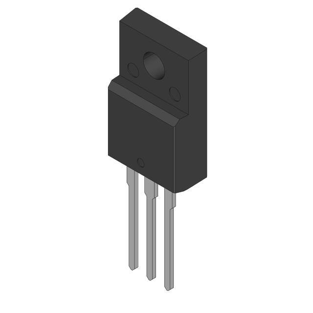
Industry standard TO-220 FULLPAK
Lead-Free
Short Circuit Rated
UltraFast IGBT
C
VCES = 600V
VCE(on) typ. = 2.21V
G
@VGE = 15V, IC = 9.2A
E
n-channel
Benefits
Generation 4 IGBTs offer highest efficiencies available
maximizing the power density of the system
IGBT's optimized for specific application conditions
HEXFREDTM diodes optimized for performance with IGBTs.
Minimized recovery characteristics reduce noise EMI
Designed to exceed the power handling capability of
equivalent industry-standard IGBT
TO-220 FULLPAK
Absolute Maximum Ratings
Parameter
VCES
IC @ TC = 25°C
IC @ TC = 100°C
ICM
ILM
IF @ TC = 100°C
IFM
tsc
VISOL
VGE
PD @ TC = 25°C
PD @ TC = 100°C
TJ
TSTG
Collector-to-Emitter Voltage
Continuous Collector Current
Continuous Collector Current
Pulsed Collector Current
Clamped Inductive Load Current
Diode Continuous Forward Current
Diode Maximum Forward Current
Short Circuit Withstand Time
RMS Isolation Voltage, Terminal to Case, t = 1 min
Gate-to-Emitter Voltage
Maximum Power Dissipation
Maximum Power Dissipation
Operating Junction and
Storage Temperature Range
Soldering Temperature, for 10 sec.
Mounting Torque, 6-32 or M3 Screw.
Max.
Units
600
17
9.2
34
34
9.2
34
10
2500
± 20
45
18
-55 to +150
V
A
µs
V
W
°C
300 (0.063 in. (1.6mm) from case)
10 lbfin (1.1 Nm)
Thermal Resistance
Parameter
RθJC
RθCS
RθJA
Wt
www.irf.com
Junction-to-Case - IGBT
Junction-to-Case - Diode
Junction-to-Ambient, typical socket mount
Weight
Typ.
Max.
2.0 (0.07)
2.8
3.7
65
Units
°C/W
g (oz)
1
06/11/2010
�IRG4IBC30KDPbF
Electrical Characteristics @ TJ = 25°C (unless otherwise specified)
V(BR)CES
∆V(BR)CES/∆TJ
VCE(on)
VGE(th)
∆VGE(th)/∆TJ
gfe
ICES
VFM
IGES
Parameter
Min. Typ. Max. Units
Collector-to-Emitter Breakdown Voltage 600
V
Temperature Coeff. of Breakdown Voltage 0.54 V/°C
Collector-to-Emitter Saturation Voltage
2.21 2.7
2.88
V
2.36
Gate Threshold Voltage
3.0
6.0
Temperature Coeff. of Threshold Voltage
-12
mV/°C
Forward Transconductance
5.4 8.1
S
Zero Gate Voltage Collector Current
250
µA
2500
Diode Forward Voltage Drop
1.4 1.7
V
1.3 1.6
Gate-to-Emitter Leakage Current
±100 nA
Conditions
VGE = 0V, IC = 250µA
VGE = 0V, IC = 1.0mA
IC = 16A
VGE = 15V
See Fig. 2, 5
IC = 28A
IC = 16A, TJ = 150°C
VCE = VGE, IC = 250µA
VCE = VGE, IC = 250µA
VCE = 100V, IC = 16A
VGE = 0V, VCE = 600V
VGE = 0V, VCE = 600V, TJ = 150°C
IC = 12A
See Fig. 13
IC = 12A, TJ = 150°C
VGE = ±20V
Switching Characteristics @ TJ = 25°C (unless otherwise specified)
Qg
Qge
Qgc
t d(on)
tr
td(off)
tf
Eon
Eoff
Ets
tsc
Parameter
Total Gate Charge (turn-on)
Gate - Emitter Charge (turn-on)
Gate - Collector Charge (turn-on)
Turn-On Delay Time
Rise Time
Turn-Off Delay Time
Fall Time
Turn-On Switching Loss
Turn-Off Switching Loss
Total Switching Loss
Short Circuit Withstand Time
t d(on)
tr
t d(off)
tf
Ets
LE
Cies
Coes
Cres
trr
Turn-On Delay Time
Rise Time
Turn-Off Delay Time
Fall Time
Total Switching Loss
Internal Emitter Inductance
Input Capacitance
Output Capacitance
Reverse Transfer Capacitance
Diode Reverse Recovery Time
Irr
Diode Peak Reverse Recovery Current
Qrr
Diode Reverse Recovery Charge
di(rec)M/dt
Diode Peak Rate of Fall of Recovery
During tb
2
Min.
10
Typ. Max. Units
Conditions
67 100
IC = 16A
11
16
nC
VCC = 400V
See Fig.8
25
37
VGE = 15V
60
42
TJ = 25°C
ns
160 250
IC = 16A, VCC = 480V
80 120
VGE = 15V, RG = 23Ω
0.60
Energy losses include "tail"
0.58
mJ and diode reverse recovery
1.18 1.6
See Fig. 9,10,14
µs
VCC = 360V, TJ = 125°C
VGE = 15V, RG = 10Ω , VCPK < 500V
58
TJ = 150°C,
See Fig. 10,11,18
42
IC = 16A, VCC = 480V
ns
210
VGE = 15V, RG = 23Ω
160
Energy losses include "tail"
1.69
mJ and diode reverse recovery
7.5
nH
Measured 5mm from package
920
VGE = 0V
110
pF
VCC = 30V
See Fig. 7
27
= 1.0MHz
42
60
ns
TJ = 25°C See Fig.
80 120
TJ = 125°C
14
IF = 12A
3.5 6.0
A
TJ = 25°C See Fig.
5.6
10
TJ = 125°C
15
VR = 200V
80 180
nC
TJ = 25°C
See Fig.
220 600
TJ = 125°C
16
di/dt = 200Aµs
180
A/µs TJ = 25°C
See Fig.
160
TJ = 125°C
17
www.irf.com
�IRG4IBC30KDPbF
12
For both:
Duty cycle: 50%
TJ = 125°C
Tsink = 90°C
Gate drive as specified
LOAD CURRENT (A)
10
8
Power Dissipation = 13 W
Square wave:
60% of rated
voltage
6
I
4
Ideal diodes
2
0
0.1
1
10
100
f, Frequency (KHz)
Fig. 1 - Typical Load Current vs. Frequency
(Load Current = IRMS of fundamental)
100
TJ = 25 o C
TJ = 150 o C
10
1
0.1
V GE = 15V
20µs PULSE WIDTH
1
10
VCE , Collector-to-Emitter Voltage (V)
Fig. 2 - Typical Output Characteristics
www.irf.com
I C , Collector-to-Emitter Current (A)
I C , Collector-to-Emitter Current (A)
100
TJ = 150 o C
10
TJ = 25 oC
1
0.1
V CC = 50V
5µs PULSE WIDTH
5
10
15
VGE , Gate-to-Emitter Voltage (V)
Fig. 3 - Typical Transfer Characteristics
3
�IRG4IBC30KDPbF
4.0
VCE , Collector-to-Emitter Voltage(V)
Maximum DC Collector Current(A)
20
15
10
5
0
25
50
75
100
125
IC = 32 A
3.0
IC = 16 A
IC = 8.0A
8A
2.0
1.0
-60 -40 -20
150
0
20
40
60
80 100 120 140 160
, Junction Temperature ( °C)
TT
J J, Junction Temperature ( °C )
TC , Case Temperature ( °C)
Fig. 4 - Maximum Collector Current vs. Case
Temperature
VGE = 15V
80 us PULSE WIDTH
Fig. 5 - Typical Collector-to-Emitter Voltage
vs. Junction Temperature
Thermal Response (Z thJC )
10
D = 0.50
1
0.20
0.10
0.05
0.1
0.01
0.00001
PDM
0.02
t1
0.01
t2
SINGLE PULSE
(THERMAL RESPONSE)
0.0001
Notes:
1. Duty factor D = t 1 / t 2
2. Peak TJ = PDM x Z thJC + TC
0.001
0.01
0.1
1
10
t1 , Rectangular Pulse Duration (sec)
Fig. 6 - Maximum Effective Transient Thermal Impedance, Junction-to-Case
4
www.irf.com
�IRG4IBC30KDPbF
1500
VGE , Gate-to-Emitter Voltage (V)
1200
C, Capacitance (pF)
20
VGE = 0V,
f = 1MHz
Cies = Cge + Cgc , Cce SHORTED
Cres = Cgc
Coes = Cce + Cgc
Cies
900
600
Coes
300
VCC = 400V
I C = 16A
16
12
8
4
Cres
0
1
10
0
100
VCE , Collector-to-Emitter Voltage (V)
10
Total Switching Losses (mJ)
Total Switching Losses (mJ)
V CC = 480V
V GE = 15V
TJ = 25 ° C
1.40 I C = 16A
1.30
1.20
1.10
10
20
30
40
R G, ,Gate
Gate Resistance
Resistance ((Ohm)
Ω)
RG
Fig. 9 - Typical Switching Losses vs. Gate
Resistance
www.irf.com
40
60
80
Fig. 8 - Typical Gate Charge vs.
Gate-to-Emitter Voltage
1.50
0
20
QG , Total Gate Charge (nC)
Fig. 7 - Typical Capacitance vs.
Collector-to-Emitter Voltage
1.00
0
50
RG = Ohm
23Ω
VGE = 15V
VCC = 480V
IC = 32 A
IC = 16 A
1
IC = 8.0A
8A
0.1
-60 -40 -20
0
20
40
60
80 100 120 140 160
TJ , Junction Temperature ( °C )
Fig. 10 - Typical Switching Losses vs.
Junction Temperature
5
�IRG4IBC30KDPbF
RG
TJ
VCC
4.0 VGE
100
Ω
= 23
Ohm
= 150 ° C
= 480V
= 15V
I C , Collector Current (A)
Total Switching Losses (mJ)
5.0
3.0
2.0
VGE = 20V
T J = 125 o C
10
1.0
0.0
0
8
16
24
32
1
40
SAFE OPERATING AREA
1
10
100
1000
VCE , Collector-to-Emitter Voltage (V)
I C , Collector-to-emitter Current (A)
Fig. 11 - Typical Switching Losses vs.
Collector-to-Emitter Current
Fig. 12 - Turn-Off SOA
Instantaneous Forward Current - I F (A)
100
TJ = 150°C
10
TJ = 125°C
TJ = 25°C
1
0.4
0.8
1.2
1.6
2.0
2.4
Forward Voltage Drop - V FM (V)
Fig. 13 - Maximum Forward Voltage Drop vs. Instantaneous Forward Current
6
www.irf.com
�IRG4IBC30KDPbF
100
160
VR = 200V
TJ = 125°C
TJ = 25°C
VR = 200V
TJ = 125°C
TJ = 25°C
120
I IRRM - (A)
t rr - (ns)
I F = 24A
I F = 12A
80
I F = 6.0A
I F = 24A
I F = 12A
10
IF = 6.0A
40
0
100
di f /dt - (A/µs)
1
100
1000
Fig. 14 - Typical Reverse Recovery vs. dif/dt
di f /dt - (A/µs)
1000
Fig. 15 - Typical Recovery Current vs. dif/dt
600
10000
VR = 200V
TJ = 125°C
TJ = 25°C
di(rec)M/dt - (A/µs)
VR = 200V
TJ = 125°C
TJ = 25°C
Q RR - (nC)
400
I F = 24A
I F = 12A
200
1000
I F = 12A
100
IF = 24A
IF = 6.0A
0
100
di f /dt - (A/µs)
Fig. 16 - Typical Stored Charge vs. dif/dt
www.irf.com
IF = 6.0A
1000
10
100
di f /dt - (A/µs)
1000
Fig. 17 - Typical di(rec)M/dt vs. dif/dt
7
�IRG4IBC30KDPbF
90% Vge
Same type
device as
D.U.T.
+Vge
Vce
430µF
80%
of Vce
D.U.T.
Ic
90% Ic
10% Vce
Ic
5% Ic
td(off)
tf
Eoff =
Fig. 18a - Test Circuit for Measurement of
ILM, Eon, Eoff(diode), trr, Qrr, Irr, td(on), tr, td(off), tf
∫
t1+5µS
Vce icIcdtdt
Vce
t1
t1
t2
Fig. 18b - Test Waveforms for Circuit of Fig. 18a, Defining
Eoff, td(off), tf
GATE VOLTAGE D.U.T.
10% +Vg
trr
Ic
Qrr =
tx
DUT VOLTAGE
AND CURRENT
Vce
10% Ic
90% Ic
tr
td(on)
10% Irr
Ipk
Vpk
Vcc
Irr
Ic
DIODE RECOVERY
WAVEFORMS
5% Vce
t1
t2
VceieIcdtdt
Eon = Vce
t1
∫
t2
DIODE REVERSE
RECOVERY ENERGY
t3
Fig. 18c - Test Waveforms for Circuit of Fig. 18a,
Defining Eon, td(on), tr
8
∫
+Vg
10% Vcc
Vcc
trr
id
Ic dtdt
tx
t4
Erec = Vd
VcidIcdt dt
t3
∫
t4
Fig. 18d - Test Waveforms for Circuit of Fig. 18a,
Defining Erec, trr, Qrr, Irr
www.irf.com
�IRG4IBC30KDPbF
Vg GATE SIGNAL
DEVICE UNDER TEST
CURRENT D.U.T.
VOLTAGE IN D.U.T.
CURRENT IN D1
t0
t1
t2
Figure 18e. Macro Waveforms for Figure 18a's Test Circuit
RL = VCC
ICM
D.U.T.
L
1000V
Vc*
50V
6000µF
100V
Figure 19. Clamped Inductive Load Test Circuit
www.irf.com
0 - VCC
480µF
Figure 20. Pulsed Collector Current
Test Circuit
9
�IRG4IBC30KDPbF
TO-220AB Full-Pak Package Outline
Dimensions are shown in millimeters (inches)
TO-220AB Full-Pak Part Marking Information
(;$03/(� 7+,6�,6�$1�,5),���*�
:,7+�$66(0%/