IXTY1R4N100P
IXTA1R4N100P
IXTP1R4N100P
PolarTM
Power MOSFET
VDSS
ID25
RDS(on)
= 1000V
= 1.4A
11.8
N-Channel Enhancement Mode
Avalanche Rated
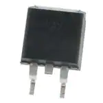
TO-252 (IXTY)
G
S
D (Tab)
TO-263 (IXTA)
Symbol
Test Conditions
Maximum Ratings
VDSS
TJ = 25C to 150C
1000
V
VDGR
TJ = 25C to 150C, RGS = 1M
1000
V
VGSS
Continuous
20
V
VGSM
Transient
30
V
ID25
TC = 25C
1.4
A
IDM
TC = 25C, Pulse Width Limited by TJM
3.0
A
IA
TC = 25C
1.4
A
EAS
TC = 25C
100
mJ
dv/dt
IS IDM, VDD VDSS, TJ 150°C
10
V/ns
PD
TC = 25C
63
W
-55 ... +150
C
TJM
150
C
Tstg
-55 ... +150
C
300
260
°C
°C
10..65 / 2.2..14.6
1.13 / 10
N/lb
Nm/lb.in
0.35
2.50
3.00
g
g
g
TJ
TL
TSOLD
Maximum Lead Temperature for Soldering
1.6 mm (0.062in.) from Case for 10s
FC
Md
Mounting Force (TO-263)
Mounting Torque (TO-220)
Weight
TO-252
TO-263
TO-220
G
S
D (Tab)
TO-220 (IXTP)
GD
G = Gate
S = Source
BVDSS
VGS = 0V, ID = 250μA
1000
VGS(th)
VDS = VGS, ID = 50μA
2.5
4.5
D
= Drain
Tab = Drain
International Standard Packages
Low QG
Avalanche Rated
Low Package Inductance
Fast Intrinsic Rectifier
Advantages
Characteristic Values
Min.
Typ.
Max.
D (Tab)
Features
Symbol
Test Conditions
(TJ = 25C, Unless Otherwise Specified)
S
High Power Density
Easy to Mount
Space Savings
V
Applications
V
DC-DC Converters
Switch-Mode and Resonant-Mode
Power Supplies
AC and DC Motor Drives
Lasers Drivers
Robotics and Servo Controls
IGSS
VGS = 20V, VDS = 0V
50 nA
IDSS
VDS = VDSS, VGS = 0V
RDS(on)
VGS = 10V, ID = 0.5 • ID25, Note 1
TJ = 125C
© 2017 IXYS CORPORATION, All Rights Reserved
5 A
150 A
11.8
DS99737C(8/17)
�IXTY1R4N100P
Symbol
Test Conditions
(TJ = 25C, Unless Otherwise Specified)
gfs
Characteristic Values
Min.
Typ.
Max
VDS = 20V, ID = 0.5 • ID25, Note 1
0.70
1.10
S
450
pF
27
pF
6
pF
17.8
nC
2.8
nC
9.9
nC
25
ns
35
ns
65
ns
28
ns
Ciss
Coss
VGS = 0V, VDS = 25V, f = 1MHz
Crss
Qg(on)
Qgs
VGS = 10V, VDS = 0.5 • VDSS, ID = 0.5 • ID25
Qgd
td(on)
tr
td(off)
tf
Resistive Switching Times
VGS = 10V, VDS = 0.5 • VDSS, ID = 0.5 • ID25
RG = 30 (External)
2.0 C/W
RthJC
RthCS
IXTA1R4N100P
IXTP1R4N100P
TO-220
C/W
0.50
Source-Drain Diode
Symbol
Test Conditions
(TJ = 25C, Unless Otherwise Specified)
Characteristic Values
Min.
Typ.
Max
IS
VGS = 0V
1.4
A
ISM
Repetitive, Pulse Width Limited by TJM
4.2
A
VSD
IF = IS, VGS = 0V, Note 1
1.5
V
trr
IF = 1.4A, -di/dt = 100A/μs, VR = 100V
750
ns
Note 1. Pulse test, t 300s, duty cycle, d 2%.
IXYS Reserves the Right to Change Limits, Test Conditions, and Dimensions.
IXYS MOSFETs and IGBTs are covered
4,835,592
by one or more of the following U.S. patents: 4,860,072
4,881,106
4,931,844
5,017,508
5,034,796
5,049,961
5,063,307
5,187,117
5,237,481
5,381,025
5,486,715
6,162,665
6,259,123B1
6,306,728B1
6,404,065B1
6,534,343
6,583,505
6,683,344
6,710,405B2
6,710,463
6,727,585
7,005,734B2
6,759,692
7,063,975B2
6,771,478B2 7,071,537
7,157,338B2
�IXTY1R4N100P
o
o
Fig. 2. Extended Output Characteristics @ TJ = 25 C
Fig. 1. Output Characteristics @ TJ = 25 C
1.4
2.2
VGS = 10V
7V
1.2
1.8
1.6
6V
I D - Amperes
I D - Amperes
VGS = 10V
7V
2.0
1.0
0.8
0.6
0.4
1.4
1.2
6V
1.0
0.8
0.6
0.4
0.2
5V
5V
0.2
0.0
0.0
0
2
4
6
8
10
12
14
0
16
5
10
15
3.0
1.4
VGS = 10V
7V
30
RDS(on) - Normalized
6V
0.8
0.6
0.4
VGS = 10V
2.6
1.0
I D - Amperes
25
Fig. 4. RDS(on) Normalized to ID = 0.7A Value vs.
Junction Temperature
o
Fig. 3. Output Characteristics @ TJ = 125 C
1.2
20
VDS - Volts
VDS - Volts
5V
0.2
2.2
I D = 1.4A
1.8
I D = 0.7A
1.4
1.0
0.6
0.0
0.2
0
5
10
15
20
25
30
35
-50
-25
0
VDS - Volts
75
100
125
150
Fig. 6. Maximum Drain Current vs. Case Temperature
TJ = 125 C
VGS = 10V
50
1.6
o
2.2
25
TJ - Degrees Centigrade
Fig. 5. RDS(on) Normalized to ID = 0.7A Value vs.
Drain Current
2.4
1.4
2.0
1.2
1.8
1.0
I D - Amperes
RDS(on) - Normalized
IXTA1R4N100P
IXTP1R4N100P
1.6
1.4
1.2
0.8
0.6
0.4
o
TJ = 25 C
0.2
1.0
0.0
0.8
0
0.2
0.4
0.6
0.8
1
1.2
1.4
I D - Amperes
© 2017 IXYS CORPORATION, All Rights Reserved
1.6
1.8
2
2.2
-50
-25
0
25
50
75
TC - Degrees Centigrade
100
125
150
�IXTY1R4N100P
Fig. 7. Input Admittance
2.0
IXTA1R4N100P
IXTP1R4N100P
Fig. 8. Transconductance
2.4
o
1.8
2.0
1.6
1.4
o
g f s - Siemens
I D - Amperes
TJ = - 40 C
VDS = 20V
VDS = 20V
1.2
1.0
o
TJ = 125 C
o
25 C
0.8
o
- 40 C
0.6
25 C
1.6
1.2
o
125 C
0.8
0.4
0.4
0.2
0.0
0.0
3.0
3.5
4.0
4.5
5.0
5.5
6.0
0
6.5
0.2
0.4
0.6
0.8
1
Fig. 9. Forward Voltage Drop of Intrinsic Diode
5.0
1.2
1.4
1.6
1.8
2
2.2
2.4
2.6
I D - Amperes
VGS - Volts
Fig. 10. Gate Charge
10
4.5
9
4.0
8
VDS = 500V
I D = 0.7A
3.5
7
3.0
6
VGS - Volts
I S - Amperes
I G = 10mA
2.5
o
TJ = 125 C
2.0
o
TJ = 25 C
1.5
5
4
3
1.0
2
0.5
1
0.0
0
0.4
0.45
0.5
0.55
0.6
0.65
0.7
0.75
0.8
0.85
0.9
0.95
0
2
4
VSD - Volts
10
12
14
16
18
10
Ciss
100
Z(th)JC - K / W
Capacitance - PicoFarads
8
Fig. 12. Maximum Transient Thermal Impedance
Fig. 11. Capacitance
1,000
6
QG - NanoCoulombs
Coss
1
0.1
10
Crss
f = 1 MHz
1
0
5
10
15
20
25
30
35
40
VDS - Volts
IXYS Reserves the Right to Change Limits, Test Conditions, and Dimensions.
0.01
0.00001
0.0001
0.001
0.01
0.1
Pulse Width - Seconds
1
10
�IXTY1R4N100P
TO-252 AA Outline
A
A
E
b3
4
L3
TO-263 Outline
E
c2
C2
TO-220 Outline
A
E1
L1
A1
L4
1
2
A2
3
L1
e
e1
e1
b2
L
L2
c
0
5.55MIN
OPTIONAL
1
1 - Gate
2,4 - Drain
3 - Source
L2
3
b2
A1
6.40
2.85MIN
2.28
1.25MIN
LAND PATTERN RECOMMENDATION
© 2017 IXYS CORPORATION, All Rights Reserved
A1
H1
Q
D2
D
b
L3
c
e
0.43 [11.0]
D1
e
E1
0
0.20 [5.0]
0.10 [2.5]
A2
EJECTOR
PIN
0.66 [16.6]
A2
1 - Gate
2,4 - Drain
3 - Source
4
A
oP
4
H
0.34 [8.7]
6.50MIN
BOTTOM
VIEW
2
E
D1
D
H
IXTA1R4N100P
IXTP1R4N100P
L1
L
0.12 [3.0]
0.06 [1.6]
e
c
e1
3X b
3X b2
1 - Gate
2,4 - Drain
3 - Source
IXYS REF: T_1R4N100P(2A) 12-19-12-B
�Disclaimer Notice - Information furnished is believed to be accurate and reliable. However, users should independently
evaluate the suitability of and test each product selected for their own applications. Littelfuse products are not designed for,
and may not be used in, all applications. Read complete Disclaimer Notice at www.littelfuse.com/disclaimer-electronics.
�


 工商网监
湘ICP备2023018690号
工商网监
湘ICP备2023018690号
