Is Now Part of
To learn more about ON Semiconductor, please visit our website at
www.onsemi.com
Please note: As part of the Fairchild Semiconductor integration, some of the Fairchild orderable part numbers
will need to change in order to meet ON Semiconductor’s system requirements. Since the ON Semiconductor
product management systems do not have the ability to manage part nomenclature that utilizes an underscore
(_), the underscore (_) in the Fairchild part numbers will be changed to a dash (-). This document may contain
device numbers with an underscore (_). Please check the ON Semiconductor website to verify the updated
device numbers. The most current and up-to-date ordering information can be found at www.onsemi.com. Please
email any questions regarding the system integration to Fairchild_questions@onsemi.com.
ON Semiconductor and the ON Semiconductor logo are trademarks of Semiconductor Components Industries, LLC dba ON Semiconductor or its subsidiaries in the United States and/or other countries. ON Semiconductor owns the rights to a number
of patents, trademarks, copyrights, trade secrets, and other intellectual property. A listing of ON Semiconductor’s product/patent coverage may be accessed at www.onsemi.com/site/pdf/Patent-Marking.pdf. ON Semiconductor reserves the right
to make changes without further notice to any products herein. ON Semiconductor makes no warranty, representation or guarantee regarding the suitability of its products for any particular purpose, nor does ON Semiconductor assume any liability
arising out of the application or use of any product or circuit, and specifically disclaims any and all liability, including without limitation special, consequential or incidental damages. Buyer is responsible for its products and applications using ON
Semiconductor products, including compliance with all laws, regulations and safety requirements or standards, regardless of any support or applications information provided by ON Semiconductor. “Typical” parameters which may be provided in ON
Semiconductor data sheets and/or specifications can and do vary in different applications and actual performance may vary over time. All operating parameters, including “Typicals” must be validated for each customer application by customer’s
technical experts. ON Semiconductor does not convey any license under its patent rights nor the rights of others. ON Semiconductor products are not designed, intended, or authorized for use as a critical component in life support systems or any FDA
Class 3 medical devices or medical devices with a same or similar classification in a foreign jurisdiction or any devices intended for implantation in the human body. Should Buyer purchase or use ON Semiconductor products for any such unintended
or unauthorized application, Buyer shall indemnify and hold ON Semiconductor and its officers, employees, subsidiaries, affiliates, and distributors harmless against all claims, costs, damages, and expenses, and reasonable attorney fees arising out
of, directly or indirectly, any claim of personal injury or death associated with such unintended or unauthorized use, even if such claim alleges that ON Semiconductor was negligent regarding the design or manufacture of the part. ON Semiconductor
is an Equal Opportunity/Affirmative Action Employer. This literature is subject to all applicable copyright laws and is not for resale in any manner.
�January 2007
FDY300NZ
tm
Single N-Channel 2.5V Specified PowerTrench MOSFET
General Description
Features
This Single N-Channel MOSFET has been designed
using Fairchild Semiconductor’s advanced Power
Trench process to optimize the RDS(ON) @ VGS = 2.5v.
• 600 mA, 20 V RDS(ON) = 700 mΩ @ VGS = 4.5 V
RDS(ON) = 850 mΩ @ VGS = 2.5 V
Applications
• ESD protection diode (note 3)
• Li-Ion Battery Pack
• RoHS Compliant
1S
G 1
G
3
S
D
2
D
Absolute Maximum Ratings
Symbol
o
TA=25 C unless otherwise noted
Parameter
VDSS
VGSS
Drain-Source Voltage
Gate-Source Voltage
ID
Drain Current
– Continuous
– Pulsed
Power Dissipation (Steady State)
PD
(Note 1a) 1a)
(Note 1a) 1a)
(Note 1b) 1
TJ, TSTG
Operating and Storage Junction Temperature
Range
Ratings
Unit
s
20
V
V
± 12
600
1000
625
446
–55 to +150
mA
mW
°C
Thermal Characteristics
RθJA
Thermal Resistance, Junction-to-Ambient
(Note 1a) 1a)
200
RθJA
Thermal Resistance, Junction-to-Ambient
(Note 1b) 1
280
°C/W
Package Marking and Ordering Information
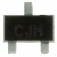
Device Marking
Device
Reel Size
Tape width
Quantity
C
FDY300NZ
7 ’’
8 mm
3000 units
2007 Fairchild Semiconductor Corporation
FDY300NZ Rev B
www.fairchildsemi.com
FDY300NZ Single N-Channel 2.5V Specified PowerTrench MOSFET
January 2007
�Symbol
TA = 25°C unless otherwise noted
Parameter
Test Conditions
Min
Typ
Max
Units
Off Characteristics
BVDSS
∆BVDSS
∆TJ
IDSS
IGSS
Drain–Source Breakdown
Voltage
Breakdown Voltage Temperature
Coefficient
Zero Gate Voltage Drain Current
Gate–Body Leakage,
On Characteristics
VGS = 0 V,
ID = 250 µA
20
V
15
ID = 250 µA, Referenced to 25°C
mV/°C
VDS = 16 V,
VGS = 0 V
VGS = ± 12 V, VDS = 0 V
VGS = ± 4.5 V, VDS = 0 V
1
± 10
±1
µA
µA
µA
1.0
3
1.3
V
mV/°C
0.24
0.36
0.70
0.35
1.8
0.70
0.85
1.25
1.00
Ω
(Note 2)
VGS(th)
∆VGS(th)
∆TJ
RDS(on)
Gate Threshold Voltage
Gate Threshold Voltage
Temperature Coefficient
Static Drain–Source
On–Resistance
gFS
Forward Transconductance
VDS = VGS,
ID = 250 µA
ID = 250 µA, Referenced to 25°C
VGS = 4.5 V,
ID = 600 mA
VGS = 2.5 V,
ID = 500 mA
ID = 150 mA
VGS = 1.8 V,
VGS = 4.5 V, ID=600mA, TJ = 125°C
VDS = 5 V,
ID = 600 mA
0.6
S
Dynamic Characteristics
Ciss
Input Capacitance
Coss
Output Capacitance
Crss
Reverse Transfer Capacitance
Switching Characteristics
td(on)
Turn–On Delay Time
tr
Turn–On Rise Time
td(off)
Turn–Off Delay Time
tf
Turn–Off Fall Time
Qg
Total Gate Charge
Qgs
Gate–Source Charge
Qgd
Gate–Drain Charge
VDS = 10 V,
f = 1.0 MHz
V GS = 0 V,
60
pF
20
pF
10
pF
(Note 2)
VDD = 10 V,
VGS = 4.5 V,
VDS = 10 V,
VGS = 4.5 V
ID = 1 A,
RGEN = 6 Ω
ID = 600 mA,
6
12
ns
8
16
ns
8
16
ns
2.4
4.8
ns
0.8
1.1
nC
0.16
nC
0.26
nC
Drain–Source Diode Characteristics and Maximum Ratings
VSD
trr
Qrr
Drain–Source Diode Forward
Voltage
Diode Reverse Recovery Time
Diode Reverse Recovery Charge
VGS = 0 V,
IS = 150 mA
IF = 600 mA,
dIF/dt = 100 A/µs
(Note 2)
0.7
1.2
8
1
V
nS
nC
Notes:
1. RθJA is the sum of the junction-to-case and case-to-ambient thermal resistance where the case thermal reference is defined as the solder mounting surface of
the drain pins. RθJC is guaranteed by design while RθCA is determined by the user's board design.
a)
200°C/W when
mounted on a 1in2 pad
of 2 oz copper
b) 280°C/W when mounted on a
minimum pad of 2 oz copper
Scale 1 : 1 on letter size paper
2. Pulse Test: Pulse Width < 300µs,
Duty Cycle < 2.0%
3. The diode connected between the gate
and source serves only as protection
againts ESD. No gate overvoltage
rating is implied.
FDY300NZ Rev B
www.fairchildsemi.com
FDY300NZ Single N-Channel 2.5V Specified PowerTrench MOSFET
Electrical Characteristics
�1
2.6
3.0V
RDS(ON), NORMALIZED
DRAIN-SOURCE ON-RESISTANCE
ID, DRAIN CURRENT (A)
VGS = 4.5V
3.5V
2.5V
0.8
2.0V
0.6
0.4
0.2
2.4
VGS = 2.0V
2.2
2
1.8
1.6
2.5V
1.4
3.0V
1.2
3.5V
4.5V
1
0.8
0
0
0.25
0.5
0.75
0
1
0.2
Figure 1. On-Region Characteristics.
0.8
1
0.9
ID = 600mA
VGS = 4.5V
ID = 300mA
RDS(ON), ON-RESISTANCE (OHM)
RDS(ON), NORMALIZED
DRAIN-SOURCE ON-RESISTANCE
0.6
Figure 2. On-Resistance Variation with
Drain Current and Gate Voltage.
1.6
1.4
1.2
1
0.8
0.6
-50
-25
0
25
50
75
100
125
0.8
0.7
0.6
TA = 125oC
0.5
0.4
0.3
TA = 25oC
0.2
150
1
2
o
TJ, JUNCTION TEMPERATURE ( C)
3
4
5
VGS, GATE TO SOURCE VOLTAGE (V)
Figure 3. On-Resistance Variation with
Temperature.
Figure 4. On-Resistance Variation with
Gate-to-Source Voltage.
1
VDS = 5V
IS, REVERSE DRAIN CURRENT (A)
1.5
ID, DRAIN CURRENT (A)
0.4
ID, DRAIN CURRENT (A)
VDS, DRAIN-SOURCE VOLTAGE (V)
25oC
o
TA = -55 C
1.2
125oC
0.9
0.6
0.3
VGS = 0V
0.1
TA = 125oC
0.01
25oC
-55oC
0.001
0.0001
0
0.5
1
1.5
2
2.5
VGS, GATE TO SOURCE VOLTAGE (V)
Figure 5. Transfer Characteristics.
FDY300NZ Rev B
3
0
0.2
0.4
0.6
0.8
1
1.2
VSD, BODY DIODE FORWARD VOLTAGE (V)
Figure 6. Body Diode Forward Voltage Variation
with Source Current and Temperature.
www.fairchildsemi.com
FDY300NZ Single N-Channel 2.5V Specified PowerTrench MOSFET
Typical Characteristics
�100
ID = 600mA
f = 1MHz
VGS = 0 V
90
4
80
VDS = 5V
CAPACITANCE (pF)
VGS, GATE-SOURCE VOLTAGE (V)
5
10V
3
15V
2
1
Ciss
70
60
50
40
Coss
30
20
10
0
Crss
0
0
0.2
0.4
0.6
0.8
1
0
4
Qg, GATE CHARGE (nC)
Figure 7. Gate Charge Characteristics.
16
20
30
P(pk), PEAK TRANSIENT POWER (W)
1ms
RDS(ON) LIMIT
1
1s
10ms
100ms
10s
DC
0.1
VGS = 4.5V
SINGLE PULSE
RθJA = 280oC/W
TA = 25oC
0.01
0.1
1
10
100
SINGLE PULSE
RθJA = 280°C/W
TA = 25°C
25
20
15
10
5
0
0.0001
0.001
0.01
0.1
1
10
100
1000
t1, TIME (sec)
VDS, DRAIN-SOURCE VOLTAGE (V)
Figure 9. Maximum Safe Operating Area.
r(t), NORMALIZED EFFECTIVE TRANSIENT
THERMAL RESISTANCE
12
Figure 8. Capacitance Characteristics.
10
ID, DRAIN CURRENT (A)
8
VDS, DRAIN TO SOURCE VOLTAGE (V)
Figure 10. Single Pulse Maximum
Power Dissipation.
1
D = 0.5
RθJA(t) = r(t) * RθJA
RθJA =280 °C/W
0.2
0.1
P(pk)
0.1
0.05
t1
t2
TJ - TA = P * RθJA(t)
Duty Cycle, D = t1 / t2
0.02
0.01
SINGLE PULSE
0.01
0.0001
0.001
0.01
0.1
1
10
100
t1, TIME (sec)
Figure 11. Transient Thermal Response Curve.
Thermal characterization performed using the conditions described in Note 1b.
Transient thermal response will change depending on the circuit board design.
FDY300NZ Rev B
www.fairchildsemi.com
1000
FDY300NZ Single N-Channel 2.5V Specified PowerTrench MOSFET
Typical Characteristics
�1.70
1.50
0.50
0.35
0.25
0.50
3
1.70
1.50
0.98
0.78
1
1.80
1.14
2
(0.15)
0.50
0.50
0.66
LAND PATTERN RECOMMENDATION
1.00
0.78
0.58
0.43
0.28
0.20
0.04
SEE DETAIL A
0.54
0.34
0.10
0.00
DETAIL A
SCALE 2 : 1
NOTES: UNLESS OTHERWISE SPECIFIED
A) THIS PACKAGE CONFORMS TO EIAJ
SC89 PACKAGING STANDARD.
B) ALL DIMENSIONS ARE IN MILLIMETERS.
C) DIMENSIONS ARE EXCLUSIVE OF BURRS,
MOLD FLASH, AND TIE BAR EXTRUSIONS.
FDY300NZ Rev B
www.fairchildsemi.com
FDY300NZ Single N-Channel 2.5V Specified PowerTrench MOSFET
Dimensional Outline and Pad Layout
�TRADEMARKS
The following are registered and unregistered tradem ark s F airc hild S em ic onduc tor owns or is authoriz ed to use and is not
intended to b e an ex haustiv e list of all suc h tradem ark s.
A C Ex ™
A c tiv eA rray ™
B ottom less™
B uild it N ow™
C oolF ET™
CROSSVOLT™
D O M E™
Ec oS P A R K ™
E2 C M O S ™
EnS igna™
F A C T®
F A S T®
F A S Tr™
FPS™
F R F ET™
F A C T Q uiet S eries™
G lob alO p toisolator™
G TO ™
H iS eC ™
I2 C ™
i-Lo ™
Im p liedD isc onnec t™
IntelliM A X ™
IS O P L A N A R ™
L ittleF ET™
M IC R O C O U P L ER ™
M ic roF ET™
M ic roP ak ™
M IC R O W IR E™
M SX™
M S X P ro™
A c ross the b oard. A round the world.™
The P ower F ranc hise®
P rogram m ab le A c tiv e D roop ™
O CX™
O C X P ro™
O P TO L O G IC ®
O P TO P L A N A R ™
PACM AN™
PO P™
P ower24 7 ™
P owerEdge™
P owerS av er™
P owerTrenc h®
Q F ET®
Q S™
Q T O p toelec tronic s™
Q uiet S eries™
R ap idC onfigure™
R ap idC onnec t™
µ S erD es™
S c alarP um p ™
S IL EN T S W ITC H ER
S M A R T S TA R T™
SPM ™
S tealth™
S up erF ET™
S up erS O T™-3
S up erS O T™-6
S up erS O T™-8
S y nc F ET™
TC M ™
Tiny B oost™
Tiny B uc k ™
Tiny P W M ™
Tiny P ower™
Tiny L ogic ®
TIN Y O P TO ™
TruTranslation™
UHC®
®
U niF ET™
VCX™
W ire™
DISC L AIMER
F A IR C H IL D S EM IC O N D U C TO R R ES ER V ES TH E R IG H T TO M A K E C H A N G ES W ITH O U T F U R TH ER N O TIC E TO A N Y P R O D U C TS
H ER EIN TO IM P R O V E R EL IA B IL ITY , F U N C TIO N O R D ES IG N . F A IR C H IL D D O ES N O T A S S U M E A N Y L IA B IL ITY A R IS IN G O U T O F TH E
A P P L IC A TIO N O R U S E O F A N Y P R O D U C T O R C IR C U IT D ES C R IB ED H ER EIN ; N EITH ER D O ES IT C O N V EY A N Y L IC EN S E U N D ER ITS
P A TEN T R IG H TS , N O R TH E R IG H TS O F O TH ER S . TH ES E S P EC IF IC A TIO N S D O N O T EX P A N D TH E TER M S O F F A IR C H IL D ’S
W O R L D W ID E TER M S A N D C O N D ITIO N S , S P EC IF IC A L L Y TH E W A R R A N TY TH ER EIN , W H IC H C O V ER S TH ES E P R O D U C TS .
L IF E SU P P O RT P O L IC Y
F A IR C H IL D ’S P R O D U C TS A R E N O T A U TH O R IZ ED F O R U S E A S C R ITIC A L C O M P O N EN TS IN L IF E S U P P O R T D EV IC ES O R S Y S TEM S
W ITH O U T TH E EX P R ES S W R ITTEN A P P R O V A L O F F A IR C H IL D S EM IC O N D U C TO R C O R P O R A TIO N .
A s used herein:
1 . L ife sup p ort dev ic es or sy stem s are dev ic es or sy stem s
whic h, (a) are intended for surgic al im p lant into the b ody , or
(b ) sup p ort or sustain life, or (c ) whose failure to p erform
when p rop erly used in ac c ordanc e with instruc tions for use
p rov ided in the lab eling, c an b e reasonab ly ex p ec ted to
result in signific ant injury to the user.�
2. A c ritic al c om p onent is any c om p onent of a life sup p ort
dev ic e or sy stem whose failure to p erform c an b e
reasonab ly ex p ec ted to c ause the failure of the life sup p ort
dev ic e or sy stem , or to affec t its safety or effec tiv eness.�
P RO DU C T STATU S DEF IN ITIO N S
De fin itio n o f Te rm s
Da ta s h e e t Id e n tific a tio n
P ro d u c t Sta tu s
De fin itio n
A dv anc e Inform ation
F orm ativ e or In
D esign
This datasheet c ontains the design sp ec ific ations for
p roduc t dev elop m ent. S p ec ific ations m ay c hange in
any m anner without notic e.
P relim inary
F irst P roduc tion
This datasheet c ontains p relim inary data, and
sup p lem entary data will b e p ub lished at a later date.
F airc hild S em ic onduc tor reserv es the right to m ak e
c hanges at any tim e without notic e in order to im p rov e
design.
N o Identific ation N eeded
F ull P roduc tion
This datasheet c ontains final sp ec ific ations. F airc hild
S em ic onduc tor reserv es the right to m ak e c hanges at
any tim e without notic e in order to im p rov e design.�
O b solete
N ot In P roduc tion
This datasheet c ontains sp ec ific ations on a p roduc t
that has b een disc ontinued b y F airc hild sem ic onduc tor.
The datasheet is p rinted for referenc e inform ation only .
R ev . I22
�ON Semiconductor and
are trademarks of Semiconductor Components Industries, LLC dba ON Semiconductor or its subsidiaries in the United States and/or other countries.
ON Semiconductor owns the rights to a number of patents, trademarks, copyrights, trade secrets, and other intellectual property. A listing of ON Semiconductor’s product/patent
coverage may be accessed at www.onsemi.com/site/pdf/Patent−Marking.pdf. ON Semiconductor reserves the right to make changes without further notice to any products herein.
ON Semiconductor makes no warranty, representation or guarantee regarding the suitability of its products for any particular purpose, nor does ON Semiconductor assume any liability
arising out of the application or use of any product or circuit, and specifically disclaims any and all liability, including without limitation special, consequential or incidental damages.
Buyer is responsible for its products and applications using ON Semiconductor products, including compliance with all laws, regulations and safety requirements or standards,
regardless of any support or applications information provided by ON Semiconductor. “Typical” parameters which may be provided in ON Semiconductor data sheets and/or
specifications can and do vary in different applications and actual performance may vary over time. All operating parameters, including “Typicals” must be validated for each customer
application by customer’s technical experts. ON Semiconductor does not convey any license under its patent rights nor the rights of others. ON Semiconductor products are not
designed, intended, or authorized for use as a critical component in life support systems or any FDA Class 3 medical devices or medical devices with a same or similar classification
in a foreign jurisdiction or any devices intended for implantation in the human body. Should Buyer purchase or use ON Semiconductor products for any such unintended or unauthorized
application, Buyer shall indemnify and hold ON Semiconductor and its officers, employees, subsidiaries, affiliates, and distributors harmless against all claims, costs, damages, and
expenses, and reasonable attorney fees arising out of, directly or indirectly, any claim of personal injury or death associated with such unintended or unauthorized use, even if such
claim alleges that ON Semiconductor was negligent regarding the design or manufacture of the part. ON Semiconductor is an Equal Opportunity/Affirmative Action Employer. This
literature is subject to all applicable copyright laws and is not for resale in any manner.
PUBLICATION ORDERING INFORMATION
LITERATURE FULFILLMENT:
Literature Distribution Center for ON Semiconductor
19521 E. 32nd Pkwy, Aurora, Colorado 80011 USA
Phone: 303−675−2175 or 800−344−3860 Toll Free USA/Canada
Fax: 303−675−2176 or 800−344−3867 Toll Free USA/Canada
Email: orderlit@onsemi.com
© Semiconductor Components Industries, LLC
N. American Technical Support: 800−282−9855 Toll Free
USA/Canada
Europe, Middle East and Africa Technical Support:
Phone: 421 33 790 2910
Japan Customer Focus Center
Phone: 81−3−5817−1050
www.onsemi.com
1
ON Semiconductor Website: www.onsemi.com
Order Literature: http://www.onsemi.com/orderlit
For additional information, please contact your local
Sales Representative
www.onsemi.com
�


 工商网监
湘ICP备2023018690号
工商网监
湘ICP备2023018690号
