Is Now Part of
To learn more about ON Semiconductor, please visit our website at
www.onsemi.com
�FDB8453LZ
N-Channel PowerTrench® MOSFET
tm
40V, 50A, 7.0m
Features
General Description
Max rDS(on) = 7.0m
at VGS = 10V, ID = 17.6A
Max rDS(on) = 9.0m
at VGS = 4.5V, ID = 14.9A
This N-Channel MOSFET is produced using Fairchild
Semiconductor’s advanced PowerTrench® process that has
been especially tailored to minimize the on-state resistance and
switching loss. G-S zener has been added to enhance ESD
voltage level.
HBM ESD protection level of 7.6kV typical (note 4)
Fast Switching
Applications
RoHS Compliant
Inverter
Power Supplies
D
D
G
G
S
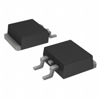
TO-263AB
FDB Series
S
MOSFET Maximum Ratings TC = 25°C unless otherwise noted
Symbol
VDS
VGS
ID
EAS
PD
TJ, TSTG
Parameter
Drain to Source Voltage
Gate to Source Voltage
Drain Current -Continuous (Package limited)
T C = 25°C
-Continuous (Silicon limited)
TC = 25°C
-Continuous
TA = 25°C
-Pulsed
Single Pulse Avalanche Energy
Power Dissipation
TC = 25°C
Power Dissipation
TA = 25°C
Operating and Storage Junction Temperature Range
(Note 1a)
(Note 3)
(Note 1a)
Ratings
40
±20
50
74
16.1
100
253
66
3.1
-55 to +150
Units
V
V
A
mJ
W
°C
Thermal Characteristics
R
R
JC
Thermal Resistance, Junction to Case
JA
Thermal Resistance, Junction to Ambient
1.88
(Note 1a)
40
°C/W
Package Marking and Ordering Information
Device Marking
FDB8453LZ
Device
FDB8453LZ
©2007 Fairchild Semiconductor Corporation
FDB8453LZ Rev.C1
Package
TO-263AB
1
Reel Size
330mm
Tape Width
24mm
Quantity
800 units
www.fairchildsemi.com
FDB8453LZ N-Channel PowerTrench® MOSFET
August 2007
�Symbol
TJ = 25°C unless otherwise noted
Parameter
Test Conditions
Min
Typ
Max
Units
Off Characteristics
BVDSS
BVDSS
TJ
IDSS
IGSS
Drain to Source Breakdown Voltage
Breakdown Voltage Temperature
Coefficient
Zero Gate Voltage Drain Current
Gate to Source Leakage Current
ID = 250 A, VGS = 0V
40
ID = 250 A, referenced to 25°C
V
36
VDS = 32V, VGS = 0V
VGS = ±20V, VDS = 0V
mV/°C
1
±10
A
A
On Characteristics
VGS(th)
VGS(th)
TJ
Gate to Source Threshold Voltage
Gate to Source Threshold Voltage
Temperature Coefficient
rDS(on)
Static Drain to Source On Resistance
gFS
Forward Transconductance
VGS = VDS, ID = 250 A
1.0
1.8
3.0
ID = 250 A, referenced to 25°C
-6.0
VGS = 10V, ID = 17.6A
VGS = 4.5V, ID = 14.9A
VGS = 10V, ID = 17.6A,
TJ = 125°C
VDS = 5V, ID = 17.6A
6.3
7.3
7.0
9.0
9.9
11
V
mV/°C
84
m
S
Dynamic Characteristics
Ciss
Coss
Crss
Rg
Input Capacitance
Output Capacitance
Reverse Transfer Capacitance
Gate Resistance
VDS = 20V, VGS = 0V,
f = 1MHz
f = 1MHz
2665
3545
pF
325
200
2.2
430
295
pF
pF
11
6
37
5
47
25
7
9
20
13
60
11
66
35
ns
ns
ns
ns
nC
nC
nC
nC
0.7
0.8
24
15
1.2
1.3
38
27
Switching Characteristics
td(on)
tr
td(off)
tf
Qg
Qg
Qgs
Qgd
Turn-On Delay Time
Rise Time
Turn-Off Delay Time
Fall Time
Total Gate Charge
Total Gate Charge
Gate to Source Charge
Gate to Drain “Miller” Charge
VDD = 20V, ID = 17.6A,
VGS = 10V, RGEN = 6
VGS = 0V to 10V
VGS = 0V to 5V
VDD = 20V,
ID = 17.6A
Drain-Source Diode Characteristics
VSD
Source to Drain Diode Forward Voltage
trr
Qrr
Reverse Recovery Time
Reverse Recovery Charge
VGS = 0V, IS = 2.6A
VGS = 0V, IS = 17.6A
(Note 2)
(Note 2)
IF = 17.6A, di/dt = 100A/ s
V
ns
nC
Notes:
1: R JA is the sum of the junction-to-case and case-to-ambient thermal resistance where the case thermal reference is defined as the solder mounting surface of the drain pins.
R JC is guaranteed by design while R JA is determined by the user’s board design.
a. 40°C/W when mounted on a 1 in2 pad of 2 oz copper
b. 62.5°C/W when mounted on a minimum pad.
2: Pulse Test: Pulse Width < 300 s, Duty cycle < 2.0%.
3: Starting TJ = 25°C, L = 3mH, IAS = 13A, VDD = 40V, VGS = 10V.
4: The diode connected between the gate and source serves only as protection against ESD. No gate overvoltage rating is implied.
©2007 Fairchild Semiconductor Corporation
FDB8453LZ Rev.C1
2
www.fairchildsemi.com
FDB8453LZ N-Channel PowerTrench® MOSFET
Electrical Characteristics
�PULSE DURATION = 80 s
DUTY CYCLE = 0.5%MAX
VGS = 10V
VGS = 4.5V
80
VGS = 4V
60
VGS = 3.5V
40
20
VGS = 3V
0
0.0
0.4
0.8
1.2
1.6
4.0
NORMALIZED
DRAIN TO SOURCE ON-RESISTANCE
ID, DRAIN CURRENT (A)
100
PULSE DURATION = 80 s
DUTY CYCLE = 0.5%MAX
3.5
VGS = 3V
3.0
VGS = 3.5V
2.5
2.0
VGS = 4V
1.5
1.0
0.5
2.0
VGS = 4.5V
0
20
VDS, DRAIN TO SOURCE VOLTAGE (V)
SOURCE ON-RESISTANCE (m )
rDS(on), DRAIN TO
NORMALIZED
DRAIN TO SOURCE ON-RESISTANCE
21
1.4
1.2
1.0
0.8
0.6
-75
-50
IS, REVERSE DRAIN CURRENT (A)
ID, DRAIN CURRENT (A)
TJ = 150oC
TJ = 25oC
TJ = -55oC
0
1
2
3
4
VGS, GATE TO SOURCE VOLTAGE (V)
12
TJ = 125oC
9
TJ = 25oC
6
2
4
6
8
10
VGS = 0V
10
TJ = 150oC
1
0.1
TJ = 25oC
0.01
TJ = -55oC
1E-3
0.0
5
0.2
0.4
0.6
0.8
1.0
1.2
VSD, BODY DIODE FORWARD VOLTAGE (V)
Figure 6. Source to Drain Diode
Forward Voltage vs Source Current
Figure 5. Transfer Characteristics
©2007 Fairchild Semiconductor Corporation
FDB8453LZ Rev.C1
15
100
60
20
PULSE DURATION = 80 s
DUTY CYCLE = 0.5%MAX
Figure 4. On-Resistance vs Gate to
Source Voltage
VDS = 5V
40
100
VGS, GATE TO SOURCE VOLTAGE (V)
PULSE DURATION = 80 s
DUTY CYCLE = 0.5%MAX
80
ID = 17.6A
18
3
-25
0
25 50 75 100 125 150
TJ, JUNCTION TEMPERATURE (oC)
Figure 3. Normalized On- Resistance
vs Junction Temperature
100
80
Figure 2. Normalized On-Resistance
vs Drain Current and Gate Voltage
ID = 17.6A
VGS = 10V
1.6
60
ID, DRAIN CURRENT (A)
Figure 1. On-Region Characteristics
1.8
40
VGS = 10V
3
www.fairchildsemi.com
FDB8453LZ N-Channel PowerTrench® MOSFET
Typical Characteristics TJ = 25°C unless otherwise noted
�4000
ID = 17.6A
Ciss
8
VDD = 15V
6
CAPACITANCE (pF)
VGS, GATE TO SOURCE VOLTAGE(V)
10
VDD = 20V
4
VDD = 25V
2
0
1000
Coss
Crss
f = 1MHz
VGS = 0V
0
10
20
30
40
100
0.1
50
Qg, GATE CHARGE (nC)
Figure 7. Gate Charge Characteristics
2
10
Ig, GATE LEAKAGE CURRENT(uA)
IAS, AVALANCHE CURRENT(A)
10
TJ = 25oC
TJ = 125oC
1
0.01
VGS = 0V
1
10
0
10
TJ = 150oC
-1
10
TJ = 25oC
-2
10
-3
10
-4
0.1
1
10
100
10
1000
0
5
10
15
20
VGS, GATE TO SOURCE VOLTAGE (V)
tAV, TIME IN AVALANCHE (ms)
Figure 9. Unclamped Inductive
Switching Capability
Figure 10. Gate Leakage Current vs Gate to
Source Voltage
80
200
100
ID, DRAIN CURRENT (A)
ID, DRAIN CURRENT (A)
40
10
Figure 8. Capacitance vs Drain
to Source Voltage
20
60
VGS = 10V
40
VGS = 4.5V
Limited by Package
20
R
0
1
VDS, DRAIN TO SOURCE VOLTAGE (V)
25
100us
10
THIS AREA IS
LIMITED BY rDS(on)
1
R
o
JC = 1.88 C/W
50
75
100
o
125
TC, CASE TEMPERATURE ( C)
0.1
0.1
150
JC
TC
10ms
DC
o
= 1.88 C/W
= 25oC
1
10
100
VDS, DRAIN to SOURCE VOLTAGE (V)
Figure 12. Forward Bias Safe
Operating Area
Figure 11. Maximum Continuous Drain
Current vs Ambient Temperature
©2007 Fairchild Semiconductor Corporation
FDB8453LZ Rev.C1
1ms
SINGLE PULSE
TJ = MAX RATED
4
www.fairchildsemi.com
FDB8453LZ N-Channel PowerTrench® MOSFET
Typical Characteristics TJ = 25°C unless otherwise noted
�P(PK), PEAK TRANSIENT POWER (W)
8000
VGS =10V
SINGLE PULSE
1000
R
JC
o
= 1.88 C/W
o
TC = 25 C
100
50
-5
10
-4
-3
10
-2
10
10
-1
10
0
1
10
10
t, PULSE WIDTH (s)
Figure 13. Single Pulse Maximum Power Dissipation
2
NORMALIZED THERMAL
IMPEDANCE, Z JC
1
0.1
DUTY CYCLE-DESCENDING ORDER
D = 0.5
0.2
0.1
0.05
0.02
0.01
PDM
t1
t2
0.01
0.005
-5
10
NOTES:
DUTY FACTOR: D = t1/t2
PEAK TJ = PDM x Z JC x R JC + TC
SINGLE PULSE
R
JC
o
= 1.88 C/W
-4
10
-3
-2
10
10
-1
10
0
10
1
10
t, RECTANGULAR PULSE DURATION (s)
Figure 14. Transient Thermal Response Curve
©2007 Fairchild Semiconductor Corporation
FDB8453LZ Rev.C1
5
www.fairchildsemi.com
FDB8453LZ N-Channel PowerTrench® MOSFET
Typical Characteristics TJ = 25°C unless otherwise noted
�The following are registered and unregistered trademarks and service marks Fairchild Semiconductor owns or is authorized to use and
is not intended to be an exhaustive list of all such trademarks.
ACEx®
Build it Now™
CorePLUS™
CROSSVOLT™
CTL™
Current Transfer Logic™
EcoSPARK®
Power247®
POWEREDGE®
Power-SPM™
PowerTrench®
Programmable Active Droop™
QFET®
QS™
QT Optoelectronics™
Quiet Series™
RapidConfigure™
SMART START™
SPM®
STEALTH™
SuperFET™
SuperSOT™-3
SuperSOT™-6
Green FPS™
Green FPS™ e-Series™
GTO™
i-Lo™
IntelliMAX™
ISOPLANAR™
MegaBuck™
MICROCOUPLER™
MicroFET™
MicroPak™
Motion-SPM™
OPTOLOGIC®
OPTOPLANAR®
®
Fairchild®
Fairchild Semiconductor®
FACT Quiet Series™
FACT®
FAST®
FastvCore™
FPS™
FRFET®
Global Power ResourceSM
®
PDP-SPM™
Power220®
SuperSOT™-8
SyncFET™
The Power Franchise®
TinyBoost™
TinyBuck™
TinyLogic®
TINYOPTO™
TinyPower™
TinyPWM™
TinyWire™
µSerDes™
UHC®
UniFET™
VCX™
DISCLAIMER
FAIRCHILD SEMICONDUCTOR RESERVES THE RIGHT TO MAKE CHANGES WITHOUT FURTHER NOTICE TO ANY PRODUCTS
HEREIN TO IMPROVE RELIABILITY, FUNCTION, OR DESIGN. FAIRCHILD DOES NOT ASSUME ANY LIABILITY ARISING OUT OF
THE APPLICATION OR USE OF ANY PRODUCT OR CIRCUIT DESCRIBED HEREIN; NEITHER DOES IT CONVEY ANY LICENSE
UNDER ITS PATENT RIGHTS, NOR THE RIGHTS OF OTHERS. THESE SPECIFICATIONS DO NOT EXPAND THE TERMS OF
FAIRCHILD’S WORLDWIDE TERMS AND CONDITIONS, SPECIFICALLY THE WARRANTY THEREIN, WHICH COVERS THESE
PRODUCTS.
LIFE SUPPORT POLICY
FAIRCHILD’S PRODUCTS ARE NOT AUTHORIZED FOR USE AS CRITICAL COMPONENTS IN LIFE SUPPORT DEVICES OR
SYSTEMS WITHOUT THE EXPRESS WRITTEN APPROVAL OF FAIRCHILD SEMICONDUCTOR CORPORATION.
As used herein:
1. Life support devices or systems are devices or systems
which, (a) are intended for surgical implant into the body, or
(b) support or sustain life, and (c) whose failure to perform
when properly used in accordance with instructions for use
provided in the labeling, can be reasonably expected to result
in significant injury to the user.
2.
A critical component is any component of a life support
device or system whose failure to perform can be reasonably
expected to cause the failure of the life support device or
system, or to affect its safety or effectiveness.
PRODUCT STATUS DEFINITIONS
Definition of Terms
Datasheet Identification
Product Status
Definition
Advance Information
Formative or In Design
This datasheet contains the design specifications for product development.
Specifications may change in any manner without notice.
Preliminary
First Production
This datasheet contains preliminary data; supplementary data will be published at a later date. Fairchild Semiconductor reserves the right to make
changes at any time without notice to improve design.
No Identification Needed
Full Production
This datasheet contains final specifications. Fairchild Semiconductor reserves
the right to make changes at any time without notice to improve design.
Obsolete
Not In Production
This datasheet contains specifications on a product that has been discontinued by Fairchild semiconductor. The datasheet is printed for reference information only.
Rev. I30
©2007 Fairchild Semiconductor Corporation
FDB8453LZ Rev.C1
6
www.fairchildsemi.com
FDB8453LZ N-Channel PowerTrench® MOSFET
TRADEMARKS
�ON Semiconductor and
are trademarks of Semiconductor Components Industries, LLC dba ON Semiconductor or its subsidiaries in the United States and/or other countries.
ON Semiconductor owns the rights to a number of patents, trademarks, copyrights, trade secrets, and other intellectual property. A listing of ON Semiconductors product/patent
coverage may be accessed at www.onsemi.com/site/pdf/Patent Marking.pdf. ON Semiconductor reserves the right to make changes without further notice to any products herein.
ON Semiconductor makes no warranty, representation or guarantee regarding the suitability of its products for any particular purpose, nor does ON Semiconductor assume any liability
arising out of the application or use of any product or circuit, and specifically disclaims any and all liability, including without limitation special, consequential or incidental damages.
Buyer is responsible for its products and applications using ON Semiconductor products, including compliance with all laws, regulations and safety requirements or standards,
regardless of any support or applications information provided by ON Semiconductor. Typical parameters which may be provided in ON Semiconductor data sheets and/or
specifications can and do vary in different applications and actual performance may vary over time. All operating parameters, including Typicals must be validated for each customer
application by customers technical experts. ON Semiconductor does not convey any license under its patent rights nor the rights of others. ON Semiconductor products are not
designed, intended, or authorized for use as a critical component in life support systems or any FDA Class 3 medical devices or medical devices with a same or similar classification
in a foreign jurisdiction or any devices intended for implantation in the human body. Should Buyer purchase or use ON Semiconductor products for any such unintended or unauthorized
application, Buyer shall indemnify and hold ON Semiconductor and its officers, employees, subsidiaries, affiliates, and distributors harmless against all claims, costs, damages, and
expenses, and reasonable attorney fees arising out of, directly or indirectly, any claim of personal injury or death associated with such unintended or unauthorized use, even if such
claim alleges that ON Semiconductor was negligent regarding the design or manufacture of the part. ON Semiconductor is an Equal Opportunity/Affirmative Action Employer. This
literature is subject to all applicable copyright laws and is not for resale in any manner.
PUBLICATION ORDERING INFORMATION
LITERATURE FULFILLMENT:
Literature Distribution Center for ON Semiconductor
19521 E. 32nd Pkwy, Aurora, Colorado 80011 USA
Phone: 303 675 2175 or 800 344 3860 Toll Free USA/Canada
Fax: 303 675 2176 or 800 344 3867 Toll Free USA/Canada
Email: orderlit@onsemi.com
Semiconductor Components Industries, LLC
N. American Technical Support: 800 282 9855 Toll Free
USA/Canada
Europe, Middle East and Africa Technical Support:
Phone: 421 33 790 2910
Japan Customer Focus Center
Phone: 81 3 5817 1050
www.onsemi.com
1
ON Semiconductor Website: www.onsemi.com
Order Literature: http://www.onsemi.com/orderlit
For additional information, please contact your local
Sales Representative
www.onsemi.com
�