MOSFET – N-Channel,
UniFETt
200 V, 16 A, 125 mW
FDD18N20LZ
Description
www.onsemi.com
UniFET MOSFET is ON Semiconductor’s high voltage MOSFET
family based on planar stripe and DMOS technology. This MOSFET
is tailored to reduce on−state resistance, and to provide better
switching performance and higher avalanche energy strength. This
device family is suitable for switching power converter applications
such as power factor correction (PFC), flat panel display (FPD) TV
power, ATX and electronic lamp ballasts.
D
G
S
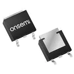
DPAK3 (TO−252 3 LD)
CASE 369AS
Features
•
•
•
•
•
•
•
MARKING DIAGRAM
RDS(on) = 125 mW (Typ.) @ VGS = 10 V, ID = 8 A
Low Gate Charge (Typ. 30 nC)
Low CRSS (Typ. 25 pF)
100% Avalanche Tested
Improved dv/dt Capability
ESD Improved Capability
These Device is Pb−Free and is RoHS Compliant
$Y&Z&3&K
FDD
18N20LZ
Applications
FDD18N20LZ
$Y
&Z
&3
&K
• LED TV
• Consumer Appliances
• Uninterruptible Power Supply
= Specific Device Code
= ON Semiconductor Logo
= Assembly Plant Code
= 3−Digit Date Code
= 2−Digits Lot run Traceability Code
D
G
S
N−Channel MOSFET
ORDERING INFORMATION
See detailed ordering and shipping information on page 6 of
this data sheet.
© Semiconductor Components Industries, LLC, 2011
September, 2020 − Rev. 3
1
Publication Order Number:
FDD18N20LZ/D
�FDD18N20LZ
MOSFET MAXIMUM RATINGS (TC = 25°C unless otherwise noted)
Symbol
FDD18N20LZ
Unit
VDSS
Drain to Source Voltage
200
V
VGSS
Gate to Source Voltage
±20
V
Continuous (TC = 25°C)
16
A
Continuous (TC = 100°C)
9.6
Pulsed
64
A
ID
Parameter
Drain Current
IDM
Drain Current (Note 1)
EAS
Single Pulsed Avalanche Energy (Note 2)
320
mJ
IAR
Avalanche Current (Note 1)
16
A
EAR
Repetitive Avalanche Energy (Note 1)
8.9
mJ
dv/dt
Peak Diode Recovery dv/dt (Note 3)
10
V/ns
(TC = 25°C)
89
W
Derate above 25°C
0.7
W/°C
−55 to +150
°C
300
°C
PD
TJ, TSTG
TL
Power Dissipation
Operating and Storage Temperature Range
Maximum Lead Temperature for Soldering, 1/8” from Case for 5 Seconds
Stresses exceeding those listed in the Maximum Ratings table may damage the device. If any of these limits are exceeded, device functionality
should not be assumed, damage may occur and reliability may be affected.
1. Repetitive rating: pulse−width limited by maximum junction temperature.
2. L = 2.5 mH, IAS = 16 A, VDD = 50 V, RG = 25 W, starting TJ = 25°C.
3. ISD ≤ 16 A, di/dt ≤ 200 A/ms, VDD ≤ BVDSS, starting TJ = 25°C.
THERMAL CHARACTERISTICS
Symbol
Parameter
FDD18N20LZ
Unit
°C/W
RqJC
Thermal Resistance, Junction to Case, Max.
1.4
RqJA
Thermal Resistance, Junction to Ambient, Max.
83
www.onsemi.com
2
�FDD18N20LZ
ELECTRICAL CHARACTERISTICS (TC = 25°C unless otherwise noted)
Symbol
Parameter
Test Condition
Min
Typ
Max
Unit
ID = 250 mA, VGS = 0 V, TJ = 25°C
200
−
−
V
ID = 250 mA, Referenced to 25°C
−
0.2
−
V/°C
VDS = 200 V, VGS = 0 V
−
−
1
mA
VDS = 160 V, TC = 125°C
−
−
10
VGS = ±16 V, VDS = 0 V
−
−
±10
mA
1.0
−
2.5
V
W
OFF CHARACTERISTICS
BVDSS
Drain to Source Breakdown Voltage
DBVDSS / D Breakdown Voltage Temperature Coefficient
TJ
DSS
Zero Gate Voltage Drain Current
IGSS
Gate to Body Leakage Current
I
ON CHARACTERISTICS
VGS(th)
Gate Threshold Voltage
VGS = VDS, ID = 250 mA
RDS(on)
Static Drain to Source On Resistance
VGS = 10 V, ID = 8 A
−
0.10
0.125
VGS = 5 V, ID = 8 A
−
0.11
0.13
VDS = 20 V, ID = 2 A
−
11
−
S
VDS = 25 V, VGS = 0 V
f = 1 MHz
−
1185
1575
pF
−
190
255
pF
−
25
40
pF
−
30
40
nC
−
3.5
−
nC
−
8.5
−
nC
−
15
40
ns
−
20
50
ns
gFS
Forward Transconductance
DYNAMIC CHARACTERISTICS
Ciss
Input Capacitance
Coss
Output Capacitance
Crss
Reverse Transfer Capacitance
Qg(tot)
Total Gate Charge at 10V
Qgs
Gate to Source Gate Charge
Qgd
Gate to Drain “Miller” Charge
VDS = 200 V, ID = 16 A, VGS = 10 V
(Note 4)
SWITCHING CHARACTERISTICS
VDD = 100 V, ID = 16 A, VGS = 10 V,
RG = 25 W (Note 4)
td(on)
Turn−On Delay Time
tr
Turn−On Rise Time
td(off)
Turn−Off Delay Time
−
135
280
ns
Turn−Off Fall Time
−
50
110
ns
Maximum Continuous Drain to Source Diode Forward Current
−
−
16
A
ISM
Maximum Pulsed Drain to Source Diode Forward Current
−
−
64
A
VSD
Drain to Source Diode Forward Voltage
VGS = 0 V, ISD = 4 A
−
−
1.4
V
trr
Reverse Recovery Time
−
105
−
ns
Qrr
Reverse Recovery Charge
VGS = 0 V, ISD = 4 A
dIF/dt = 100 A/ms
−
0.4
−
mC
tf
DAIN−SOURCE DIODE CHARACTERISTICS
IS
Product parametric performance is indicated in the Electrical Characteristics for the listed test conditions, unless otherwise noted. Product
performance may not be indicated by the Electrical Characteristics if operated under different conditions.
4. Essentially independent of operating temperature typical characteristics.
www.onsemi.com
3
�FDD18N20LZ
TYPICAL PERFORMANCE CHARACTERISTICS
100
VGS = 10 V
7V
5V
4.5 V
4V
3.5 V
3V
10
ID, Drain Current [A]
ID, Drain Current [A]
100
1
10
150°C
25°C
1
*Notes:
1. VDS = 20 V
−55°C 2. 250 ms Pulse Test
*Notes:
1. 250 ms Pulse Test
2. TC = 25°C
0.1
0.01
0.1
1
0.1
10
0
VDS, Drain−Source Voltage [V]
0.36
8
100
IS, Reverse Drain Current [A]
RDS(on),Drain−Source On−Resistance [W]
6
Figure 2. Transfer Characteristics
0.30
0.24
VGS = 10 V
0.18
VGS = 20 V
0.12
150°C
10
25°C
*Note: TJ = 25°C
0
10
20
30
40
50
1
0.4
60
ID, Drain Current [A]
0.8
1.0
1.2
1.4
1.6
1.8
VGS, Gate−Source Voltage [V]
10
1000
10
0.1
0.6
Figure 4. Body Diode Forward Voltage
Variation vs. Source Current and Temperature
5000
100
*Notes:
1. VGS = 0 V
2. 250 ms Pulse Test
VSD, Body Diode Forward Voltage [V]
Figure 3. On−Resistance Variation vs.
Drain Current and Gate Voltage
Capacitances [pF]
4
VGS, Gate−Source Voltage [V]
Figure 1. On−Region Characteristics
0.06
2
Ciss
Coss
*Note:
1. VGS = 0 V
2. f = 1 MHz
Ciss = Cgs + Cgd (Cds = shorted)
Coss = Cds + Cgd
Crss = Cgd
1
Crss
10
VDS = 50 V
VDS = 100 V
VDS = 160 V
8
6
4
2
0
30
VDS, Drain−Source Voltage [V]
*Note: ID = 16 A
0
7
14
21
28
Qg, Total Voltage Charge [nC]
Figure 5. Capacitance Characteristics
Figure 6. Gate Charge Characteristics
www.onsemi.com
4
35
�FDD18N20LZ
2.4
1.15
RDS(on),Drain−Source On−Resistance
[Normalized]
BVDSS,Drain−Source Breakdown Voltage
[Normalized]
TYPICAL PERFORMANCE CHARACTERISTICS (Continued)
1.10
1.05
1.00
0.95
*Notes:
1. VGS = 0 V
2. ID = 250 ms
0.90
0.85
−80
−40
0
40
80
120
2.0
1.6
1.2
0.4
−80
160
TJ, Junction Temperature [°C]
40
80
120
160
16
100 ms
Operation in this
Area is Limited
by RDS(ON)
*Notes:
1. TC = 25°C
2. TJ = 150°C
3. Single Pulse
1
1 ms
10 ms
DC
10
100
12
ID, Drain Current [A]
30 ms
10
8
4
0
25
1000
VDS, Drain−Source Voltage [V]
50
75
100
125
TC, Case Temperature [°C]
Figure 9. Maximum Safe Operating Area
Figure 10. Maximum Drain Current vs.
Case Temperature
2
ZqJC(t), Thermal Response [°C/W]
ID, Drain Current [A]
0
Figure 8. On−Resistance Variation vs.
Temperature
100
0.1
0.1
−40
TJ, Junction Temperature [°C]
Figure 7. Breakdown Voltage Variation vs.
Temperature
1
*Notes:
1. VGS = 10 V
2. ID = 8 A
0.8
1
0.5
0.2
PDM
0.1
0.1
t1
0.05
0.02
0.01
Single pulse
0.01 −5
10
t2
*Notes:
1. ZqJC(t) = 1.4°C/W Max.
2. Duty Factor, D = t1 / t2
3. TJM − TC = PDM x ZqJC(t)
10
−4
10
−3
10
−2
t1, Rectangular Pulse Duration [s]
Figure 11. Transient Thermal Response Curve
www.onsemi.com
5
10
−1
1
150
�FDD18N20LZ
PACKAGE MARKING ANDORDERING INFORMATION
Part Number
FDD18N20LZ
Top Mark
Package
Reel Size
Tape Width
Shipping†
FDD18N20LZ
DPAK3 (TO−252 3 LD)
(Pb−Free)
330 mm
16 mm
2500 / Tape & Reel
†For information on tape and reel specifications, including part orientation and tape sizes, please refer to our Tape and Reel Packaging
Specifications Brochure, BRD8011/D.
UniFET is trademark of Semiconductor Components Industries, LLC (SCILLC) or its subsidiaries in the United States and/or other countries.
www.onsemi.com
6
�MECHANICAL CASE OUTLINE
PACKAGE DIMENSIONS
DPAK3 (TO−252 3 LD)
CASE 369AS
ISSUE O
DOCUMENT NUMBER:
DESCRIPTION:
98AON13810G
DPAK3 (TO−252 3 LD)
DATE 30 SEP 2016
Electronic versions are uncontrolled except when accessed directly from the Document Repository.
Printed versions are uncontrolled except when stamped “CONTROLLED COPY” in red.
PAGE 1 OF 1
ON Semiconductor and
are trademarks of Semiconductor Components Industries, LLC dba ON Semiconductor or its subsidiaries in the United States and/or other countries.
ON Semiconductor reserves the right to make changes without further notice to any products herein. ON Semiconductor makes no warranty, representation or guarantee regarding
the suitability of its products for any particular purpose, nor does ON Semiconductor assume any liability arising out of the application or use of any product or circuit, and specifically
disclaims any and all liability, including without limitation special, consequential or incidental damages. ON Semiconductor does not convey any license under its patent rights nor the
rights of others.
© Semiconductor Components Industries, LLC, 2019
www.onsemi.com
�ON Semiconductor and
are trademarks of Semiconductor Components Industries, LLC dba ON Semiconductor or its subsidiaries in the United States and/or other countries.
ON Semiconductor owns the rights to a number of patents, trademarks, copyrights, trade secrets, and other intellectual property. A listing of ON Semiconductor’s product/patent
coverage may be accessed at www.onsemi.com/site/pdf/Patent−Marking.pdf. ON Semiconductor reserves the right to make changes without further notice to any products herein.
ON Semiconductor makes no warranty, representation or guarantee regarding the suitability of its products for any particular purpose, nor does ON Semiconductor assume any liability
arising out of the application or use of any product or circuit, and specifically disclaims any and all liability, including without limitation special, consequential or incidental damages.
Buyer is responsible for its products and applications using ON Semiconductor products, including compliance with all laws, regulations and safety requirements or standards,
regardless of any support or applications information provided by ON Semiconductor. “Typical” parameters which may be provided in ON Semiconductor data sheets and/or
specifications can and do vary in different applications and actual performance may vary over time. All operating parameters, including “Typicals” must be validated for each customer
application by customer’s technical experts. ON Semiconductor does not convey any license under its patent rights nor the rights of others. ON Semiconductor products are not
designed, intended, or authorized for use as a critical component in life support systems or any FDA Class 3 medical devices or medical devices with a same or similar classification
in a foreign jurisdiction or any devices intended for implantation in the human body. Should Buyer purchase or use ON Semiconductor products for any such unintended or unauthorized
application, Buyer shall indemnify and hold ON Semiconductor and its officers, employees, subsidiaries, affiliates, and distributors harmless against all claims, costs, damages, and
expenses, and reasonable attorney fees arising out of, directly or indirectly, any claim of personal injury or death associated with such unintended or unauthorized use, even if such
claim alleges that ON Semiconductor was negligent regarding the design or manufacture of the part. ON Semiconductor is an Equal Opportunity/Affirmative Action Employer. This
literature is subject to all applicable copyright laws and is not for resale in any manner.
PUBLICATION ORDERING INFORMATION
LITERATURE FULFILLMENT:
Email Requests to: orderlit@onsemi.com
ON Semiconductor Website: www.onsemi.com
◊
TECHNICAL SUPPORT
North American Technical Support:
Voice Mail: 1 800−282−9855 Toll Free USA/Canada
Phone: 011 421 33 790 2910
www.onsemi.com
1
Europe, Middle East and Africa Technical Support:
Phone: 00421 33 790 2910
For additional information, please contact your local Sales Representative
�