ON Semiconductor
Is Now
To learn more about onsemi™, please visit our website at
www.onsemi.com
onsemi and and other names, marks, and brands are registered and/or common law trademarks of Semiconductor Components Industries, LLC dba “onsemi” or its affiliates and/or
subsidiaries in the United States and/or other countries. onsemi owns the rights to a number of patents, trademarks, copyrights, trade secrets, and other intellectual property. A listing of onsemi
product/patent coverage may be accessed at www.onsemi.com/site/pdf/Patent-Marking.pdf. onsemi reserves the right to make changes at any time to any products or information herein, without
notice. The information herein is provided “as-is” and onsemi makes no warranty, representation or guarantee regarding the accuracy of the information, product features, availability, functionality,
or suitability of its products for any particular purpose, nor does onsemi assume any liability arising out of the application or use of any product or circuit, and specifically disclaims any and all
liability, including without limitation special, consequential or incidental damages. Buyer is responsible for its products and applications using onsemi products, including compliance with all laws,
regulations and safety requirements or standards, regardless of any support or applications information provided by onsemi. “Typical” parameters which may be provided in onsemi data sheets and/
or specifications can and do vary in different applications and actual performance may vary over time. All operating parameters, including “Typicals” must be validated for each customer application
by customer’s technical experts. onsemi does not convey any license under any of its intellectual property rights nor the rights of others. onsemi products are not designed, intended, or authorized
for use as a critical component in life support systems or any FDA Class 3 medical devices or medical devices with a same or similar classification in a foreign jurisdiction or any devices intended for
implantation in the human body. Should Buyer purchase or use onsemi products for any such unintended or unauthorized application, Buyer shall indemnify and hold onsemi and its officers, employees,
subsidiaries, affiliates, and distributors harmless against all claims, costs, damages, and expenses, and reasonable attorney fees arising out of, directly or indirectly, any claim of personal injury or death
associated with such unintended or unauthorized use, even if such claim alleges that onsemi was negligent regarding the design or manufacture of the part. onsemi is an Equal Opportunity/Affirmative
Action Employer. This literature is subject to all applicable copyright laws and is not for resale in any manner. Other names and brands may be claimed as the property of others.
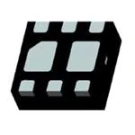
�Dual N-Channel PowerTrench MOSFET
Features
General Description
x 3.7 A, 20V.
This device is designed specifically as a single package
RDS(ON) = 86 m: @ VGS = 2.5V
x Low profile – 0.8 mm maximum – in the new package
solution for dual switching requirements in cellular
handset
and
other
ultra-portable
applications.
It
MicroFET 2x2 mm
x HBM ESD protection level > 2kV (Note 3)
features two independent N-Channel MOSFETs with
low on-state resistance for minimum conduction losses.
x RoHS Compliant
The MicroFET 2x2 package offers exceptional thermal
Free from halogenated compounds and antimony
oxides
performance for its physical size and is well suited to
linear mode applications.
PIN 1
S1 G1
D1
RDS(ON) = 68 m: @ VGS = 4.5V
D2
D2
D1 G2 S2
S1
1
6
D1
G1
2
5
G2
D2
3
4
S2
MicroFET 2x2
Absolute Maximum Ratings
Symbol
VDS
TA=25oC unless otherwise noted
Parameter
Drain-Source Voltage
Gate-Source Voltage
VGS
Drain Current
ID
– Continuous
V
r12
V
A
3.7
(Note 1a)
1.4
(Note 1b)
0.7
6
Power Dissipation for Single Operation
Operating and Storage Junction Temperature Range
TJ, TSTG
Units
20
(Note 1a)
– Pulsed
PD
Ratings
W
–55 to +150
qC
Thermal Characteristics
RTJA
Thermal Resistance, Junction-to-Ambient
(Note 1a)
86 (Single Operation)
RTJA
Thermal Resistance, Junction-to-Ambient
(Note 1b)
173 (Single Operation)
RTJA
Thermal Resistance, Junction-to-Ambient
(Note 1c)
69 (Dual Operation)
RTJA
Thermal Resistance, Junction-to-Ambient
(Note 1d)
151 (Dual Operation)
qC/W
Package Marking and Ordering Information
Device Marking
Device
Reel Size
Tape width
Quantity
028
FDMA1028NZ
7’’
8mm
3000 units
20�3 Semiconductor Components Industries, LLC.
October-2017, Rev. 2
Publication Order Number:
FDMA1028NZ/D
FDMA1028NZ Dual N-Channel PowerTrench MOSFET
FDMA1028NZ
�Symbol
Parameter
TA = 25°C unless otherwise noted
Test Conditions
Min Typ Max Units
Off Characteristics
BVDSS
'BVDSS
���'TJ
IDSS
IGSS
Drain–Source Breakdown Voltage
Breakdown Voltage Temperature
Coefficient
ID = 250 PA
VGS = 0 V,
ID = 250 PA, Referenced to 25qC
V
20
mV/qC
15
Zero Gate Voltage Drain Current
VDS = 16 V,
VGS = 0 V
1
PA
Gate–Body Leakage
VGS = ± 12 V,
VDS = 0 V
±10
PA
On Characteristics
(Note 2)
0.6
1.0
1.5
V
VGS(th)
'VGS(th)
���'TJ
RDS(on)
Gate Threshold Voltage
Gate Threshold Voltage
Temperature Coefficient
Static Drain–Source
On–Resistance
ID = 250 PA
VDS = VGS,
ID = 250 PA, Referenced to 25qC
VGS = 4.5 V,
ID = 3.7 A
ID = 3.3 A
VGS = 2.5 V,
VGS= 4.5 V, ID = 3.7 A, TJ=125qC
37
50
53
gFS
Forward Transconductance
VDS = 10 V,
ID = 3.7 A
16
S
VDS = 10 V,
f = 1.0 MHz
V GS = 0 V,
340
pF
80
pF
mV/qC
–4
68
86
90
m:
Dynamic Characteristics
Ciss
Input Capacitance
Coss
Output Capacitance
Crss
Reverse Transfer Capacitance
Rg
Gate Resistance
Switching Characteristics
td(on)
Turn–On Delay Time
tr
Turn–On Rise Time
60
pF
25
Ω
(Note 2)
VDD = 10 V,
VGS = 4.5 V,
ID = 1 A,
RGEN = 6 :
8
16
ns
8
16
ns
td(off)
Turn–Off Delay Time
14
26
ns
tf
Turn–Off Fall Time
3
6
ns
Qg
Total Gate Charge
4
6
Qgs
Gate–Source Charge
Qgd
Gate–Drain Charge
VDS = 10 V,
VGS = 4.5 V
ID = 3.7 A,
www.onsemi.com
2
nC
0.7
nC
1.1
nC
FDMA1028NZ Dual N-Channel PowerTrench MOSFET
Electrical Characteristics
�Notes:
1. RθJA is determined with the device mounted on a 1 in2 oz. copper pad on a 1.5 x 1.5 in. board of FR-4 material. RθJC is guaranteed by design while RθJA is determined by the
user's board design.
(a) RθJA = 86 °C/W when mounted on a 1 in2 pad of 2 oz copper, 1.5 " x 1.5 " x 0.062 " thick PCB. For single operation.
(b) RθJA = 173 °C/W when mounted on a minimum pad of 2 oz copper. For single operation.
(c) RθJA = 69 oC/W when mounted on a 1 in2 pad of 2 oz copper, 1.5 ” x 1.5 ” x 0.062 ” thick PCB. For dual operation.
(d) RθJA = 151 oC/W when mounted on a minimum pad of 2 oz copper. For dual operation.
a. 86 °C/W when mounted on
a 1 in2 pad of 2 oz copper
b. 173 °C/W when mounted on
a minimum pad of 2 oz copper
c. 69 °C/W when mounted on
a 1 in2 pad of 2 oz copper
d. 151 °C/W when mounted on
a minimum pad of 2 oz copper
2. Pulse Test : Pulse Width < 300 us, Duty Cycle < 2.0%
3. The diode connected between the gate and source serves only as protection against ESD. No gate overvoltage rating is implied.
www.onsemi.com
3
FDMA1028NZ Dual N-Channel PowerTrench MOSFET
Electrical Characteristics TJ = 25 °C unless otherwise noted
�6
2
2.0V
RDS(ON), NORMALIZED
DRAIN-SOURCE ON-RESISTANCE
2.5V
VGS = 4.5V
ID, DRAIN CURRENT (A)
5
3.5V
3.0V
4
3
2
1
1.5V
0
0.2
0.4
0.6
0.8
VDS, DRAIN-SOURCE VOLTAGE (V)
1
1.4
2.5V
1.2
3.0V
3.5V
4.0V
1
1.2
0
4.5V
1
2
3
4
ID, DRAIN CURRENT (A)
5
6
Figure 2. On-Resistance Variation with
Drain Current and Gate Voltage.
Figure 1. On-Region Characteristics.
0.13
1.6
ID = 3.7A
VGS = 4.5V
1.5
ID = 1.85A
RDS(ON), ON-RESISTANCE (OHM)
RDS(ON), NORMALIZED
DRAIN-SOURCE ON-RESISTANCE
1.6
0.8
0
1.4
1.3
1.2
1.1
1
0.9
0.8
0.11
0.09
o
0.07
TA = 125 C
0.05
o
TA = 25 C
0.7
0.6
0.03
-50
-25
0
25
50
75
100
o
TJ, JUNCTION TEMPERATURE ( C)
125
150
0
Figure 3. On-Resistance Variation with
Temperature.
2
4
6
8
VGS, GATE TO SOURCE VOLTAGE (V)
10
Figure 4. On-Resistance Variation with
Gate-to-Source Voltage.
100
6
VGS = 0V
IS, REVERSE DRAIN CURRENT (A)
VDS = 5V
5
ID, DRAIN CURRENT (A)
VGS = 2.0V
1.8
4
3
2
o
TA = 125 C
-55oC
1
o
10
1
0.1
TA = 125oC
0.01
o
25 C
o
0.001
-55 C
25 C
0.0001
0
0.5
1
1.5
2
VGS, GATE TO SOURCE VOLTAGE (V)
Figure 5. Transfer Characteristics.
2.5
0
0.2
0.4
0.6
0.8
1
VSD, BODY DIODE FORWARD VOLTAGE (V)
1.2
Figure 6. Body Diode Forward Voltage Variation
with Source Current and Temperature.
www.onsemi.com
4
FDMA1028NZ Dual N-Channel PowerTrench MOSFET
Typical Characteristics
�10
500
VDS = 5V
VGS, GATE-SOURCE VOLTAGE (V)
ID = 3.7A
f = 1MHz
VGS = 0 V
15V
8
400
CAPACITANCE (pF)
10V
6
4
300
200
Coss
2
100
0
0
Crss
0
4
6
Qg, GATE CHARGE (nC)
2
8
10
0
Figure 7. Gate Charge Characteristics.
RDS(ON) LIMIT
100us
1ms
10ms
100ms
1s
10s
DC
1
VGS = 4.5V
SINGLE PULSE
RTJA = 173°C/W
TA = 25°C
0.1
0.1
1
10
VDS, DRAIN-SOURCE VOLTAGE (V)
SINGLE PULSE
RTJA = 173°C/W
TA = 25°C
40
30
20
10
0.01
100
Figure 9. Maximum Safe Operating Area.
r(t), NORMALIZED EFFECTIVE TRANSIENT
THERMAL RESISTANCE
20
50
P(pk), PEAK TRANSIENT POWER (W)
10
5
10
15
VDS, DRAIN TO SOURCE VOLTAGE (V)
Figure 8. Capacitance Characteristics.
100
ID, DRAIN CURRENT (A)
Ciss
0
0.0001
0.001
0.01
0.1
1
t1, TIME (sec)
10
100
Figure 10. Single Pulse Maximum Power
Dissipation.
1
D = 0.5
RTJA(t) = r(t) * RTJA
RTJA =173 °C/W
0.2
0.1
P(pk)
0.1
0.05
t1
0.02
0.01
t2
TJ - TA = P * RTJA(t)
Duty Cycle, D = t1 / t2
SINGLE PULSE
0.01
0.0001
0.001
0.01
0.1
1
10
t1, TIME (sec)
Figure 11. Transient Thermal Response Curve.
Thermal characterization performed using the conditions described in Note 1b.
Transient thermal response will change depending on the circuit board design.
www.onsemi.com
5
100
1000
1000
FDMA1028NZ Dual N-Channel PowerTrench MOSFET
Typical Characteristics
�FDMA1028NZ Dual N-Channel PowerTrench MOSFET
Dimensional Outline and Pad Layout
Package drawings are provided as a service to customers considering ON Semiconductor components. Drawings may change in
any manner without notice. Please note the revision and/or date on the drawing and contact a ON Semiconductor representative to
verify or obtain the most recent revision. Package specifications do not expand the terms of ON Semiconductor’s worldwide terms
and conditions, specifically the warranty therein, which covers ON Semiconductor products.
www.onsemi.com
6
�ON Semiconductor and
are trademarks of Semiconductor Components Industries, LLC dba ON Semiconductor or its subsidiaries in the United States and/or other countries.
ON Semiconductor owns the rights to a number of patents, trademarks, copyrights, trade secrets, and other intellectual property. A listing of ON Semiconductor’s product/patent
coverage may be accessed at www.onsemi.com/site/pdf/Patent−Marking.pdf. ON Semiconductor reserves the right to make changes without further notice to any products herein.
ON Semiconductor makes no warranty, representation or guarantee regarding the suitability of its products for any particular purpose, nor does ON Semiconductor assume any liability
arising out of the application or use of any product or circuit, and specifically disclaims any and all liability, including without limitation special, consequential or incidental damages.
Buyer is responsible for its products and applications using ON Semiconductor products, including compliance with all laws, regulations and safety requirements or standards,
regardless of any support or applications information provided by ON Semiconductor. “Typical” parameters which may be provided in ON Semiconductor data sheets and/or
specifications can and do vary in different applications and actual performance may vary over time. All operating parameters, including “Typicals” must be validated for each customer
application by customer’s technical experts. ON Semiconductor does not convey any license under its patent rights nor the rights of others. ON Semiconductor products are not
designed, intended, or authorized for use as a critical component in life support systems or any FDA Class 3 medical devices or medical devices with a same or similar classification
in a foreign jurisdiction or any devices intended for implantation in the human body. Should Buyer purchase or use ON Semiconductor products for any such unintended or unauthorized
application, Buyer shall indemnify and hold ON Semiconductor and its officers, employees, subsidiaries, affiliates, and distributors harmless against all claims, costs, damages, and
expenses, and reasonable attorney fees arising out of, directly or indirectly, any claim of personal injury or death associated with such unintended or unauthorized use, even if such
claim alleges that ON Semiconductor was negligent regarding the design or manufacture of the part. ON Semiconductor is an Equal Opportunity/Affirmative Action Employer. This
literature is subject to all applicable copyright laws and is not for resale in any manner.
PUBLICATION ORDERING INFORMATION
LITERATURE FULFILLMENT:
Literature Distribution Center for ON Semiconductor
19521 E. 32nd Pkwy, Aurora, Colorado 80011 USA
Phone: 303−675−2175 or 800−344−3860 Toll Free USA/Canada
Fax: 303−675−2176 or 800−344−3867 Toll Free USA/Canada
Email: orderlit@onsemi.com
❖
© Semiconductor Components Industries, LLC
N. American Technical Support: 800−282−9855 Toll Free
USA/Canada
Europe, Middle East and Africa Technical Support:
Phone: 421 33 790 2910
Japan Customer Focus Center
Phone: 81−3−5817−1050
ON Semiconductor Website: www.onsemi.com
Order Literature: http://www.onsemi.com/orderlit
For additional information, please contact your local
Sales Representative
www.onsemi.com
�


 工商网监
湘ICP备2023018690号
工商网监
湘ICP备2023018690号
