Silicon Carbide Schottky
Diode
1200 V, 20 A
FFSB20120A-F085
Description
Silicon Carbide (SiC) Schottky Diodes use a completely new
technology that provides superior switching performance and higher
reliability compared to Silicon. No reverse recovery current,
temperature independent switching characteristics, and excellent
thermal performance sets Silicon Carbide as the next generation of
power semiconductor. System benefits include highest efficiency,
faster operating frequency, increased power density, reduced EMI, and
reduced system size and cost.
www.onsemi.com
1.,3. Cathode
2. Anode
Schottky Diode
Features
•
•
•
•
•
•
•
Max Junction Temperature 175°C
Avalanche Rated 200 mJ
High Surge Current Capacity
Positive Temperature Coefficient
Ease of Paralleling
No Reverse Recovery/No Forward Recovery
AEC−Q101 qualified
3
1
2
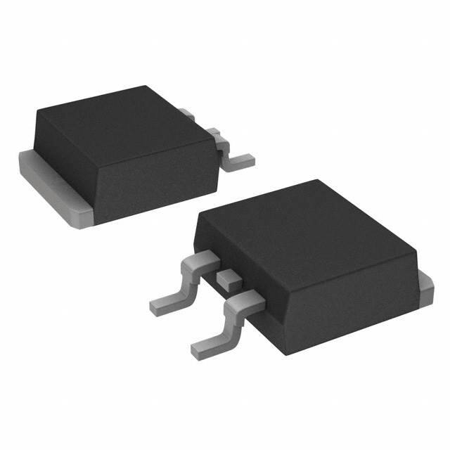
D2PAK2 (TO−263−2L)
CASE 418BK
MARKING DIAGRAM
Applications
• Automotive HEV−EV Onboard Chargers
• Automotive HEV−EV DC−DC Converters
$Y&Z&3&K
FFSB
20120A
$Y
&Z
&3
&K
FFSB20120A
= ON Semiconductor Logo
= Assembly Plant Code
= Numeric Date Code
= Lot Code
= Specific Device Code
ORDERING INFORMATION
See detailed ordering and shipping information on page 2
of this data sheet.
© Semiconductor Components Industries, LLC, 2013
August, 2020 − Rev. 1
1
Publication Order Number:
FFSB20120A−F085/D
�FFSB20120A−F085
ABSOLUTE MAXIMUM RATINGS (TC = 25°C unless otherwise noted)
Parameter
Symbol
Ratings
Unit
1200
V
200
mJ
A
VRRM
Peak Repetitive Reverse Voltage
EAS
Single Pulse Avalanche Energy
IF
Continuous Rectified Forward Current @ TC < 157°C
20
Continuous Rectified Forward Current @ TC < 135°C
32
IF, Max
(Note 1)
Non−Repetitive Peak Forward Surge Current
TC = 25°C, 10 ms
1190
TC = 150°C, 10 ms
990
A
IF, SM
Non−Repetitive Forward Surge Current
Half−Sine Pulse, tp = 8.3 ms
135
A
IF, RM
Repetitive Forward Surge Current
Half−Sine Pulse, tp = 8.3 ms
74
A
Ptot
Power Dissipation
TC = 25°C
333
W
TC = 150°C
55
W
−55 to +175
°C
TJ, TSTG
Operating and Storage Temperature Range
Stresses exceeding those listed in the Maximum Ratings table may damage the device. If any of these limits are exceeded, device functionality
should not be assumed, damage may occur and reliability may be affected.
THERMAL CHARACTERISTICS
Symbol
RqJC
Parameter
Thermal Resistance, Junction to Case, Max
Ratings
Unit
0.45
°C/W
PACKAGE MARKING AND ORDERING INFORMATION
Part Number
Top Mark
Package
Shipping†
FFSB20120A−F085
FFSB20120A
D2PAK
800 Units/
Tape & Reel
†For information on tape and reel specifications, including part orientation and tape sizes, please refer to our Tape and Reel Packaging
Specifications Brochure, BRD8011/D.
ELECTRICAL CHARACTERISTICS (TC = 25°C unless otherwise noted)
Symbol
VF
IR
Parameter
Forward Voltage
Reverse Current
Test Conditions
Min
Typ.
Max.
Unit
IF = 20 A, TC = 25°C
−
1.45
1.75
V
IF = 20 A, TC = 125°C
−
1.7
2
IF = 20 A, TC = 175°C
−
2
2.4
VR = 1200 V, TC = 25°C
−
−
200
VR = 1200 V, TC = 125°C
−
−
300
VR = 1200 V, TC = 175°C
−
−
400
mA
QC
Total Capacitive Charge
V = 800 V
−
120
−
nC
C
Total Capacitance
VR = 1 V, f = 100 kHz
−
1220
−
pF
VR = 400 V, f = 100 kHz
−
111
−
VR = 800 V, f = 100 kHz
−
88
−
Product parametric performance is indicated in the Electrical Characteristics for the listed test conditions, unless otherwise noted. Product
performance may not be indicated by the Electrical Characteristics if operated under different conditions.
1. EAS of 200 mJ is based on starting TJ = 25°C, L = 0.5 mH, IAS = 29 A, V = 50 V.
www.onsemi.com
2
�FFSB20120A−F085
TYPICAL CHARACTERISTICS (TC = 25°C unless otherwise noted)
101
TJ = −55°C
TJ = 25°C
TJ = 75°C
16
IR, REVERSE CURRENT (mA)
IF, FORWARD CURRENT (A)
20
12
TJ = 125°C
TJ = 175°C
8
4
0
0.0
0.5
1.0
1.5
2.0
VF, FORWARD VOLTAGE (V)
2.5
100
TJ = 175°C
10−1
TJ = 125°C
TJ = 75°C
10−2
TJ = 25°C
10−3
200
3.0
Figure 1. Forward Characteristics
200
D = 0.2
D = 0.3
150
D = 0.5
100
50
D=1
D = 0.7
50
75
125
100
150
300
250
200
150
100
50
0
25
175
TC, CASE TEMPERATURE (5C)
50
75
100
125
150
175
TC, CASE TEMPERATURE (5C)
Figure 3. Current Derating
Figure 4. Power Derating
150
5000
125
CAPACITIANCE (pF)
QC, CAPACITIVE CHARGE (nC)
1200
350
D = 0.1
0
25
400
600
800
1000
VR, REVERSE VOLTAGE (V)
Figure 2. Reverse Characteristics
PTOT, POWER DISSIPATION (W)
IP, PEAK FORWARD CURRENT (A)
250
TJ = −55°C
100
75
50
25
0
1000
100
0
200
400
600
800
50
0.1
1000
VR, REVERSE VOLTAGE (V)
Figure 5. Capacitive Charge vs. Reverse Voltage
1
10
100
VR, REVERSE VOLTAGE (V)
1000
Figure 6. Capacitive Charge vs. Reverse Voltage
www.onsemi.com
3
�FFSB20120A−F085
TYPICAL CHARACTERISTICS (TC = 25°C unless otherwise noted) (continued)
EC, CAPACITIVE ENERGY (mJ)
50
40
30
20
10
0
0
200
400
800
600
1000
VR, REVERSE VOLTAGE (V)
r(t), NORMALIZED EFFECTIVE TRANSIENT
THERMAL RESISTANCE
Figure 7. Capacitance Stored Energy
2
1
DUTY CYCLE − DESCENDING ORDER
PDM
0.1
0.2
0.5
0.1
0.0
1
0.02
0.01
t1
t2
0.05
NOTES:
ZqJC (t) = r(t) × RqJC
RqJC = 0.45°C/W
PEAK TJ = PDM × ZqJC (t) + TC
Duty cycle, D = t1/t2
0.001
SINGLE PULSE
0.0001
10−6
10−5
10−4
10−3
10−2
10−1
1
t, RECTANGULAR PULSE DURATION (sec)
Figure 8. Junction−to−Case Transient Thermal Response Curve
TEST CIRCUIT AND WAVEFORMS
L = 0.5 mH
R < 0.1 W
VDD = 50 V
EAVL = 1/2LI2 [VR(AVL) / (VR(AVL) − VDD)]
Q1 = IGBT (BVCES > DUT VR(AVL))
L
Q1
CURRENT
SENSE
DUT
VAVL
R
+
VDD
IL
IL
I V
VDD
−
t0
t1
Figure 9. Unclamped Inductive Switching Test Circuit & Waveform
www.onsemi.com
4
t2
t
�MECHANICAL CASE OUTLINE
PACKAGE DIMENSIONS
D2PAK2 (TO−263−2L)
CASE 418BK
ISSUE O
DATE 02 AUG 2018
GENERIC
MARKING DIAGRAM*
XXXXXXXXG
AYWW
XXX = Specific Device Code
A
= Assembly Location
Y
= Year
WW = Work Week
G = Pb−Free Package
*This information is generic. Please refer to
device data sheet for actual part marking.
Pb−Free indicator, “G” or microdot “ G”,
may or may not be present. Some products
may not follow the Generic Marking.
DOCUMENT NUMBER:
DESCRIPTION:
98AON93788G
D2PAK2 (TO−263−2L)
Electronic versions are uncontrolled except when accessed directly from the Document Repository.
Printed versions are uncontrolled except when stamped “CONTROLLED COPY” in red.
PAGE 1 OF 1
ON Semiconductor and
are trademarks of Semiconductor Components Industries, LLC dba ON Semiconductor or its subsidiaries in the United States and/or other countries.
ON Semiconductor reserves the right to make changes without further notice to any products herein. ON Semiconductor makes no warranty, representation or guarantee regarding
the suitability of its products for any particular purpose, nor does ON Semiconductor assume any liability arising out of the application or use of any product or circuit, and specifically
disclaims any and all liability, including without limitation special, consequential or incidental damages. ON Semiconductor does not convey any license under its patent rights nor the
rights of others.
© Semiconductor Components Industries, LLC, 2018
www.onsemi.com
�onsemi,
, and other names, marks, and brands are registered and/or common law trademarks of Semiconductor Components Industries, LLC dba “onsemi” or its affiliates
and/or subsidiaries in the United States and/or other countries. onsemi owns the rights to a number of patents, trademarks, copyrights, trade secrets, and other intellectual property.
A listing of onsemi’s product/patent coverage may be accessed at www.onsemi.com/site/pdf/Patent−Marking.pdf. onsemi reserves the right to make changes at any time to any
products or information herein, without notice. The information herein is provided “as−is” and onsemi makes no warranty, representation or guarantee regarding the accuracy of the
information, product features, availability, functionality, or suitability of its products for any particular purpose, nor does onsemi assume any liability arising out of the application or use
of any product or circuit, and specifically disclaims any and all liability, including without limitation special, consequential or incidental damages. Buyer is responsible for its products
and applications using onsemi products, including compliance with all laws, regulations and safety requirements or standards, regardless of any support or applications information
provided by onsemi. “Typical” parameters which may be provided in onsemi data sheets and/or specifications can and do vary in different applications and actual performance may
vary over time. All operating parameters, including “Typicals” must be validated for each customer application by customer’s technical experts. onsemi does not convey any license
under any of its intellectual property rights nor the rights of others. onsemi products are not designed, intended, or authorized for use as a critical component in life support systems
or any FDA Class 3 medical devices or medical devices with a same or similar classification in a foreign jurisdiction or any devices intended for implantation in the human body. Should
Buyer purchase or use onsemi products for any such unintended or unauthorized application, Buyer shall indemnify and hold onsemi and its officers, employees, subsidiaries, affiliates,
and distributors harmless against all claims, costs, damages, and expenses, and reasonable attorney fees arising out of, directly or indirectly, any claim of personal injury or death
associated with such unintended or unauthorized use, even if such claim alleges that onsemi was negligent regarding the design or manufacture of the part. onsemi is an Equal
Opportunity/Affirmative Action Employer. This literature is subject to all applicable copyright laws and is not for resale in any manner.
PUBLICATION ORDERING INFORMATION
LITERATURE FULFILLMENT:
Email Requests to: orderlit@onsemi.com
onsemi Website: www.onsemi.com
◊
TECHNICAL SUPPORT
North American Technical Support:
Voice Mail: 1 800−282−9855 Toll Free USA/Canada
Phone: 011 421 33 790 2910
Europe, Middle East and Africa Technical Support:
Phone: 00421 33 790 2910
For additional information, please contact your local Sales Representative
�


 工商网监
湘ICP备2023018690号
工商网监
湘ICP备2023018690号
