MMPQ2222A
Preferred Device
Quad General Purpose Transistor
NPN Silicon
http://onsemi.com
MAXIMUM RATINGS
Rating Collector − Emitter Voltage Collector − Base Voltage Emitter − Base Voltage Collector Current − Continuous Symbol VCEO VCB VEB IC Value 40 75 5.0 500 Four Transistors Equal Power Total Power Dissipation @ TA = 25°C Derate above 25°C Total Power Dissipation @ TC = 25°C Derate above 25°C Operating and Storage Junction Temperature Range PD Watts 1.0 8.0 2.4 19.2 −55 to +150 mW/°C Watts mW/°C °C Unit Vdc Vdc Vdc mAdc
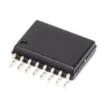
1 2 3 4 5 6 7 8
16 15 14 13 12 11 10 9
PD
TJ, Tstg
SO−16 CASE 751B STYLE 4
Maximum ratings are those values beyond which device damage can occur. Maximum ratings applied to the device are individual stress limit values (not normal operating conditions) and are not valid simultaneously. If these limits are exceeded, device functional operation is not implied, damage may occur and reliability may be affected.
MARKING DIAGRAM
MMPQ2222A AWLYWW
MMPQ2222A ic Device Code A sembly Location WL Lot Y WW Week Device MMPQ2222A
= Specif= As= Wafer = Year = Work
ORDERING INFORMATION
Package SO−16 Shipping 48 Units/Rail
Preferred devices are recommended choices for future use and best overall value.
© Semiconductor Components Industries, LLC, 2006
August, 2006 − Rev. 2
1
Publication Order Number: MMPQ2222A/D
�MMPQ2222A
ELECTRICAL CHARACTERISTICS (TA = 25°C unless otherwise noted)
Characteristic Symbol Min Typ Max Unit
OFF CHARACTERISTICS
Collector − Emitter Breakdown Voltage (Note 1) (IC = 10 mAdc, IB = 0) Collector − Base Breakdown Voltage (IC = 10 mAdc, IE = 0) Emitter − Base Breakdown Voltage (IB = 10 mAdc, IC = 0) Collector Cutoff Current (VCB = 50 Vdc, IE = 0) (VCB = 60 Vdc, IE = 0) Emitter Cutoff Current (VEB = 3.0 Vdc, IC = 0) V(BR)CEO V(BR)CBO V(BR)EBO ICBO 40 75 5.0 − − − − − − − − − − − − − − − 50 10 100 nAdc Vdc Vdc Vdc nAdc
IEBO
ON CHARACTERISTICS
DC Current Gain (Note 1) (IC = 100 mA, VCE = 10 V) (IC = 1.0 mA, VCE = 10 V) (IC = 10 mA, VCE = 10 V) (IC = 150 mA, VCE = 10 V) (IC = 500 mA, VCE = 10 V) (IC = 150 mA, VCE = 1.0 V) Collector − Emitter Saturation Voltage (Note 1) (IC = 150 mAdc, IB = 15 mAdc) (IC = 500 mAdc, IB = 50 mAdc) Base − Emitter Saturation Voltage (Note 1) (IC = 150 mAdc, IB = 15 mAdc) (IC = 500 mAdc, IB = 50 mAdc) hFE − 35 50 75 100 40 50 − − − − − − − − − − − − − − − − − 300 − − Vdc 0.3 1.0 Vdc 1.2 2.0
VCE(sat)
VBE(sat)
DYNAMIC CHARACTERISTICS
Current − Gain − Bandwidth Product (Note 1) (IC = 20 mAdc, VCE = 20 Vdc, f = 100 MHz) Output Capacitance (VCB = 10 Vdc, IE = 0, f = 1.0 MHz) Input Capacitance (VEB = 0.5 Vdc, IC = 0, f = 1.0 MHz) fT Cob Cib 200 − − 350 4.5 17 − − − MHz pF pF
SWITCHING CHARACTERISTICS
Turn−On Time (VCC = 30 Vdc, VBE(off) = −0.5 Vdc, IC = 150 mAdc, IB1 = 15 mAdc) Turn−Off Time (VCC = 30 Vdc, IC = 150 mAdc, IB1 = IB2 = 15 mAdc) 1. Pulse Test: Pulse Width ≤ 300 ms, Duty Cycle ≤ 2%. ton − 25 − ns
toff
−
250
−
ns
http://onsemi.com
2
�MMPQ2222A
SWITCHING TIME EQUIVALENT TEST CIRCUITS
+30 V +16 V 0 −2 V 1.0 to 100 μs, DUTY CYCLE ≈ 2.0% 1 kΩ < 2 ns 200 +16 V 0 CS* < 10 pF −14 V < 20 ns 1.0 to 100 μs, DUTY CYCLE ≈ 2.0% 1k 1N914 +30 V 200
CS* < 10 pF
−4 V Scope rise time < 4 ns *Total shunt capacitance of test jig, connectors, and oscilloscope.
Figure 1. Turn−On Time
Figure 2. Turn−Off Time
1000 700 500 hFE , DC CURRENT GAIN 300 200
TJ = 125°C
25°C 100 70 50 30 20 10 0.1 0.2 0.3 0.5 0.7 1.0 2.0 −55°C VCE = 1.0 V VCE = 10 V 3.0 5.0 7.0 10 20 IC, COLLECTOR CURRENT (mA) 30 50 70 100 200 300 500 700 1.0 k
Figure 3. DC Current Gain
VCE , COLLECTOR−EMITTER VOLTAGE (VOLTS)
1.0 TJ = 25°C 0.8 IC = 1.0 mA
0.6
10 mA
150 mA
500 mA
0.4
0.2 0 0.005
0.01
0.02 0.03
0.05
0.1
0.2 0.3 0.5 1.0 IB, BASE CURRENT (mA)
2.0
3.0
5.0
10
20
30
50
Figure 4. Collector Saturation Region
http://onsemi.com
3
�MMPQ2222A
200 100 70 50 t, TIME (ns) 30 20 10 7.0 5.0 3.0 2.0 5.0 7.0 10 200 300 20 30 50 70 100 IC, COLLECTOR CURRENT (mA) 500 IC/IB = 10 TJ = 25°C tr @ VCC = 30 V td @ VEB(off) = 2.0 V td @ VEB(off) = 0 500 300 200 100 70 50 30 20 10 7.0 5.0 t′s = ts − 1/8 tf VCC = 30 V IC/IB = 10 IB1 = IB2 TJ = 25°C
t, TIME (ns)
tf
5.0 7.0 10
20 30 50 70 100 200 IC, COLLECTOR CURRENT (mA)
300
500
Figure 5. Turn − On Time
Figure 6. Turn − Off Time
10 8.0 IC = 1.0 mA, RS = 150 Ω 500 μA, RS = 200 Ω 100 μA, RS = 2.0 kΩ 50 μA, RS = 4.0 kΩ RS = OPTIMUM RS = SOURCE RS = RESISTANCE
10 f = 1.0 kHz 8.0 NF, NOISE FIGURE (dB) IC = 50 μA 100 μA 500 μA 1.0 mA
NF, NOISE FIGURE (dB)
6.0
6.0
4.0
4.0
2.0 0 0.01 0.02 0.05 0.1 0.2
2.0 0 50
0.5 1.0 2.0
5.0 10
20
50 100
100 200
500 1.0 k 2.0 k
5.0 k 10 k 20 k
50 k 100 k
f, FREQUENCY (kHz)
RS, SOURCE RESISTANCE (OHMS)
Figure 7. Frequency Effects
f T, CURRENT−GAIN BANDWIDTH PRODUCT (MHz)
Figure 8. Source Resistance Effects
30 20 CAPACITANCE (pF) Ceb 10 7.0 5.0 Ccb 3.0 2.0 0.1
500 VCE = 20 V TJ = 25°C
300 200
100 70 50 1.0 2.0 3.0 5.0 7.0 10 20 30 IC, COLLECTOR CURRENT (mA) 50 70 100
0.2 0.3
0.5 0.7 1.0 2.0 3.0 5.0 7.0 10 REVERSE VOLTAGE (VOLTS)
20 30
50
Figure 9. Capacitances
Figure 10. Current−Gain Bandwidth Product
http://onsemi.com
4
�MMPQ2222A
1.0 TJ = 25°C 0.8 VBE(sat) @ IC/IB = 10 0.6 VBE(on) @ VCE = 10 V 0.4 COEFFICIENT (mV/ °C) V, VOLTAGE (VOLTS) 1.0 V 0 −0.5 −1.0 −1.5 −2.0 VCE(sat) @ IC/IB = 10 0 0.1 0.2 50 100 200 0.5 1.0 2.0 5.0 10 20 IC, COLLECTOR CURRENT (mA) 500 1.0 k −2.5 0.1 0.2 0.5 1.0 2.0 5.0 10 20 50 100 200 IC, COLLECTOR CURRENT (mA) 500 RqVB for VBE RqVC for VCE(sat) +0.5
0.2
Figure 11. “On” Voltages
Figure 12. Temperature Coefficients
http://onsemi.com
5
�MMPQ2222A
PACKAGE DIMENSIONS
SO−16 CASE 751B−05 ISSUE J
− A−
16 9 NOTES: 1. DIMENSIONING AND TOLERANCING PER ANSI Y14.5M, 1982. 2. CONTROLLING DIMENSION: MILLIMETER. 3. DIMENSIONS A AND B DO NOT INCLUDE MOLD PROTRUSION. 4. MAXIMUM MOLD PROTRUSION 0.15 (0.006) PER SIDE. 5. DIMENSION D DOES NOT INCLUDE DAMBAR PROTRUSION. ALLOWABLE DAMBAR PROTRUSION SHALL BE 0.127 (0.005) TOTAL IN EXCESS OF THE D DIMENSION AT MAXIMUM MATERIAL CONDITION. DIM A B C D F G J K M P R MILLIMETERS MIN MAX 9.80 10.00 3.80 4.00 1.35 1.75 0.35 0.49 0.40 1.25 1.27 BSC 0.19 0.25 0.10 0.25 0_ 7_ 5.80 6.20 0.25 0.50 INCHES MIN MAX 0.386 0.393 0.150 0.157 0.054 0.068 0.014 0.019 0.016 0.049 0.050 BSC 0.008 0.009 0.004 0.009 0_ 7_ 0.229 0.244 0.010 0.019
− B−
1 8
P
8 PL
0.25 (0.010)
M
B
S
G F
K C −T−
SEATING PLANE
R
X 45 _
M D
16 PL M
J
0.25 (0.010)
TB
S
A
S
SOLDERING FOOTPRINT
0.060 1.52
STYLE 4: PIN 1. 2. 3. 4. 5. 6. 7. 8. 9. 10. 11. 12. 13. 14. 15. 16.
COLLECTOR, DYE #1 COLLECTOR, #1 COLLECTOR, #2 COLLECTOR, #2 COLLECTOR, #3 COLLECTOR, #3 COLLECTOR, #4 COLLECTOR, #4 BASE, #4 EMITTER, #4 BASE, #3 EMITTER, #3 BASE, #2 EMITTER, #2 BASE, #1 EMITTER, #1
0.275 7.0
0.155 4.0
0.024 0.6
0.050 1.270
inches mm
ON Semiconductor and are registered trademarks of Semiconductor Components Industries, LLC (SCILLC). SCILLC reserves the right to make changes without further notice to any products herein. SCILLC makes no warranty, representation or guarantee regarding the suitability of its products for any particular purpose, nor does SCILLC assume any liability arising out of the application or use of any product or circuit, and specifically disclaims any and all liability, including without limitation special, consequential or incidental damages. “Typical” parameters which may be provided in SCILLC data sheets and/or specifications can and do vary in different applications and actual performance may vary over time. All operating parameters, including “Typicals” must be validated for each customer application by customer’s technical experts. SCILLC does not convey any license under its patent rights nor the rights of others. SCILLC products are not designed, intended, or authorized for use as components in systems intended for surgical implant into the body, or other applications intended to support or sustain life, or for any other application in which the failure of the SCILLC product could create a situation where personal injury or death may occur. Should Buyer purchase or use SCILLC products for any such unintended or unauthorized application, Buyer shall indemnify and hold SCILLC and its officers, employees, subsidiaries, affiliates, and distributors harmless against all claims, costs, damages, and expenses, and reasonable attorney fees arising out of, directly or indirectly, any claim of personal injury or death associated with such unintended or unauthorized use, even if such claim alleges that SCILLC was negligent regarding the design or manufacture of the part. SCILLC is an Equal Opportunity/Affirmative Action Employer. This literature is subject to all applicable copyright laws and is not for resale in any manner.
PUBLICATION ORDERING INFORMATION
LITERATURE FULFILLMENT: Literature Distribution Center for ON Semiconductor P.O. Box 5163, Denver, Colorado 80217 USA Phone: 303−675−2175 or 800−344−3860 Toll Free USA/Canada Fax: 303−675−2176 or 800−344−3867 Toll Free USA/Canada Email: orderlit@onsemi.com N. American Technical Support: 800−282−9855 Toll Free USA/Canada Europe, Middle East and Africa Technical Support: Phone: 421 33 790 2910 Japan Customer Focus Center Phone: 81−3−5773−3850 ON Semiconductor Website: www.onsemi.com Order Literature: http://www.onsemi.com/orderlit For additional information, please contact your local Sales Representative
http://onsemi.com
6
MMPQ2222A/D
�


 工商网监
湘ICP备2023018690号
工商网监
湘ICP备2023018690号
