NSS12100UW3TCG
12 V, 1 A, Low VCE(sat)
PNP Transistor
ON Semiconductor’s e2 PowerEdge family of low VCE(sat)
transistors are miniature surface mount devices featuring ultra low
saturation voltage (VCE(sat)) and high current gain capability. These
are designed for use in low voltage, high speed switching applications
where affordable efficient energy control is important.
Typical application are DC−DC converters and power management
in portable and battery powered products such as cellular and cordless
phones, PDAs, computers, printers, digital cameras and MP3 players.
Other applications are low voltage motor controls in mass storage
products such as disc drives and tape drives. In the automotive
industry they can be used in air bag deployment and in the instrument
cluster. The high current gain allows e2PowerEdge devices to be
driven directly from PMU’s control outputs, and the Linear Gain
(Beta) makes them ideal components in analog amplifiers.
http://onsemi.com
12 VOLTS, 1.0 AMPS
PNP LOW VCE(sat) TRANSISTOR
EQUIVALENT RDS(on) 400 mW
COLLECTOR
3
1
BASE
Features
•
•
•
•
•
•
•
High Current Capability (1 A)
High Power Handling (Up to 740 mW)
Low VCE(s) (200 mV Typical @ 500 mA)
Small Size
Low Noise
NSV Prefix for Automotive and Other Applications Requiring
Unique Site and Control Change Requirements; AEC−Q101
Qualified and PPAP Capable
These Devices are Pb−Free, Halogen Free/BFR Free and are RoHS
Compliant
2
EMITTER
3
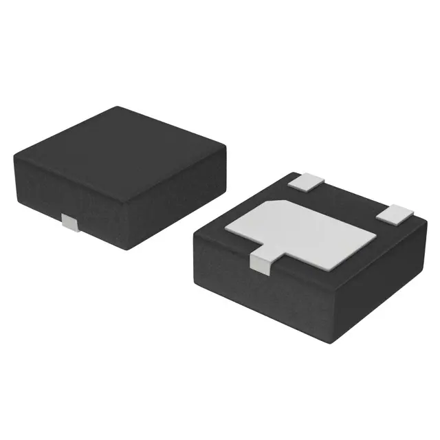
WDFN3
CASE 506AU
2
1
MARKING DIAGRAM
VG M
G
Benefits
• High Specific Current and Power Capability Reduces Required PCB Area
• Reduced Parasitic Losses Increases Battery Life
1
VG = Specific Device Code
M = Date Code
G
= Pb−Free Package
MAXIMUM RATINGS (TA = 25°C)
Symbol
Max
Unit
Collector-Emitter Voltage
VCEO
−12
Vdc
Collector-Base Voltage
VCBO
−12
Vdc
Device
Package
Shipping†
Emitter-Base Voltage
VEBO
−5.0
Vdc
NSS12100UW3TCG
WDFN3
(Pb−Free)
3000/
Tape & Reel
Collector Current − Continuous
Collector Current − Peak
IC
ICM
−1.0
−2.0
Adc
NSV12100UW3TCG
WDFN3
(Pb−Free)
3000/
Tape & Reel
Electrostatic Discharge
ESD
HBM Class 3B
MM Class C
Rating
Stresses exceeding those listed in the Maximum Ratings table may damage the
device. If any of these limits are exceeded, device functionality should not be
assumed, damage may occur and reliability may be affected.
© Semiconductor Components Industries, LLC, 2014
September, 2014 − Rev. 1
1
ORDERING INFORMATION
†For information on tape and reel specifications,
including part orientation and tape sizes, please
refer to our Tape and Reel Packaging Specifications
Brochure, BRD8011/D.
Publication Order Number:
NSS12100UW3/D
�NSS12100UW3TCG
THERMAL CHARACTERISTICS
Characteristic
Total Device Dissipation, TA = 25°C
Derate above 25°C
Thermal Resistance, Junction−to−Ambient
Total Device Dissipation, TA = 25°C
Derate above 25°C
Symbol
Max
Unit
PD (Note 1)
740
6.0
mW
mW/°C
RqJA (Note 1)
169
°C/W
PD (Note 2)
1.1
9.0
W
mW/°C
RqJA (Note 2)
110
°C/W
Thermal Resistance, Junction−to−Lead 6
RqJL (Note 2)
33
°C/W
Junction and Storage Temperature Range
TJ, Tstg
−55 to +150
°C
Thermal Resistance, Junction−to−Ambient
1. FR− 4 @ 100 mm2, 1 oz copper traces.
2. FR− 4 @ 500 mm2, 1 oz copper traces.
ELECTRICAL CHARACTERISTICS (TJ = 25°C unless otherwise noted)
Symbol
Min
Typ
Max
Unit
Collector −Emitter Breakdown Voltage, (IC = −10 mAdc, IB = 0)
V(BR)CEO
−12
−
−
Vdc
Collector −Base Breakdown Voltage, (IC = −0.1 mAdc, IE = 0)
V(BR)CBO
−12
−
−
Vdc
Emitter −Base Breakdown Voltage, (IE = −0.1 mAdc, IC = 0)
V(BR)EBO
−5.0
−
−
Vdc
Collector Cutoff Current, (VCB = −12 Vdc, IE = 0)
ICBO
−
−0.02
−0.1
mAdc
Emitter Cutoff Current, (VCES = −5.0 Vdc, IE = 0)
IEBO
−
−0.03
−0.1
mAdc
200
100
75
−
−
−
400
250
−
−
−
−
−
−
−0.030
−0.080
−0.050
−0.200
−0.400
−0.040
−0.100
−0.060
−0.225
−0.440
−
−0.95
−1.15
−
−1.05
−1.20
Characteristic
OFF CHARACTERISTICS
ON CHARACTERISTICS
hFE
DC Current Gain (Note 3)
(IC = −10 mA, VCE = −2.0 V)
(IC = −500 mA, VCE = −2.0 V)
(IC = −1.0 A, VCE = −2.0 V)
Collector −Emitter Saturation Voltage (Note 3)
(IC = −0.05 A, IB = −0.005 A) (Note 4)
(IC = −0.1 A, IB = −0.002 A)
(IC = −0.1 A, IB = −0.010 A)
(IC = −0.5 A, IB = −0.050 A)
(IC = −1.0 A, IB = −0.100 A)
VCE(sat)
Base −Emitter Saturation Voltage (Note 3)
(IC = −1.0 A, IB = −0.01 A)
VBE(sat)
Base −Emitter Turn−on Voltage (Note 3)
(IC = −2.0 A, VCE = −1.0 V)
VBE(on)
V
V
V
Input Capacitance (VEB = −0.5 V, f = 1.0 MHz)
Cibo
−
40
50
pF
Output Capacitance (VCB = −3.0 V, f = 1.0 MHz)
Cobo
−
15
20
pF
Delay (VCC = −10 V, IC = 750 mA, IB1 = 15 mA)
td
−
−
20
ns
Rise (VCC = −10 V, IC = 750 mA, IB1 = 15 mA)
tr
−
−
90
ns
Storage (VCC = −10 V, IC = 750 mA, IB1 = 15 mA)
ts
−
−
140
ns
Fall (VCC = −10 V, IC = 750 mA, IB1 = 15 mA)
tf
−
−
100
ns
Current −Gain − Bandwidth Product, (IC = −100 mA, VCE = −5 Vdc, f = 100 MHz)
fT
200
−
−
MHz
Noise Figure, (IC = −0.2 mA, VCE = −5 Vdc, RS = 2 kW, f = 1 kHz, BW = 200Hz)
NF
−
−
5.0
dB
SWITCHING CHARACTERISTICS
SMALL− SIGNAL CHARACTERISTICS
Product parametric performance is indicated in the Electrical Characteristics for the listed test conditions, unless otherwise noted. Product
performance may not be indicated by the Electrical Characteristics if operated under different conditions.
3. Pulsed Condition: Pulse Width = 300 msec, Duty Cycle ≤ 2%.
4. Guaranteed by design but not tested.
http://onsemi.com
2
�NSS12100UW3TCG
0.9
3.0
IC/IB = 10
VCE(sat) = 150°C
VCE(sat), COLLECTOR EMITTER
SATURATION VOLTAGE (V)
VCE(sat), COLLECTOR EMITTER
SATURATION VOLTAGE (V)
1.0
25°C
0.8
0.7
−55°C
0.6
0.5
0.4
0.3
0.2
0.1
0.01
0.1
1
IC, COLLECTOR CURRENT (A)
0.001
2.5
2.0
150°C
1.5
1.0
0.5
10
0.001
Figure 1. Collector Emitter Saturation Voltage vs.
Collector Current
VBE(sat), BASE EMITTER
SATURATION VOLTAGE (V)
hFE, DC CURRENT GAIN
IC/IB = 10
500
150°C (2.0 V)
25°C (5.0 V)
25°C (2.0 V)
−55°C (5.0 V)
200
−55°C (2.0 V)
100
1.2
1.0
TA = −55°C
0.8
0.6
25°C
0.4
150°C
0.2
0
0
0.001
0.01
0.1
1
0.001
10
IC, COLLECTOR CURRENT (A)
VCE, COLLECTOR−EMITTER VOLTAGE (V)
VCE = −1.0 V
1.2
1.0
TA = −55°C
0.8
25°C
0.4
150°C
0.2
0
0.01
0.1
0.1
1
10
Figure 4. Base Emitter Saturation Voltage vs.
Collector Current
1.4
0.001
0.01
IC, COLLECTOR CURRENT (A)
Figure 3. DC Current Gain vs. Collector
Current
VBE(on), BASE EMITTER TURN−ON VOLTAGE (V)
10
1.4
150°C (5.0 V)
0.6
0.01
0.1
1
IC, COLLECTOR CURRENT (A)
Figure 2. Collector Emitter Saturation Voltage vs.
Collector Current
600
300
25°C
0
0
400
VCE(sat) = −55°C
IC/IB = 100
10
1
1.0
10 mA
100 mA
300 mA
IC = 500 mA
0.8
0.6
0.4
0.2
0
0.01
IC, COLLECTOR CURRENT (A)
0.1
1
10
IB, BASE CURRENT (mA)
Figure 5. Base Emitter Turn−On Voltage vs.
Collector Current
Figure 6. Saturation Region
http://onsemi.com
3
100
�NSS12100UW3TCG
30
Cobo, OUTPUT CAPACITANCE (pF)
Cibo, INPUT CAPACITANCE (pF)
50
45
40
Cibo(pF)
35
30
25
20
0
1
2
3
4
VEB, EMITTER BASE VOLTAGE (V)
5
25
Cobo(pF)
20
15
10
5
0
0
Figure 7. Input Capacitance
1
2
3
4
5
6
7
8
VCB, COLLECTOR BASE VOLTAGE (V)
Figure 8. Output Capacitance
http://onsemi.com
4
9
10
�MECHANICAL CASE OUTLINE
PACKAGE DIMENSIONS
WDFN3 2x2, 1.3P
CASE 506AU
ISSUE A
DATE 18 AUG 2016
1
SCALE 4:1
D
NOTES:
1. DIMENSIONING AND TOLERANCING PER ASME Y14.5M, 1994 .
2. CONTROLLING DIMENSION: MILLIMETERS.
3. DIMENSION b APPLIES TO PLATED TERMINAL AND IS
MEASURED BETWEEN 0.25 AND 0.30 MM FROM TERMINAL.
4. COPLANARITY APPLIES TO THE EXPOSED PAD AS WELL AS
THE TERMINALS.
A
B
PIN ONE
REFERENCE
2X
0.10 C
2X
0.10 C
ÇÇÇÇ
ÇÇÇÇ
ÇÇÇÇ
ÇÇÇÇ
DIM
A
A1
A3
b
D
D2
E
E2
e
K
L
E
MIN
0.70
0.00
0.25
1.40
0.90
0.35
MILLIMETERS
NOM
MAX
0.75
0.80
0.05
0.20 REF
0.30
0.35
2.00 BSC
1.50
1.60
2.00 BSC
1.00
1.10
1.30 BSC
0.35 REF
0.40
0.45
MIN
0.028
0.000
INCHES
NOM
0.030
0.008 REF
0.012
0.079 BSC
0.055
0.059
0.079 BSC
0.035
0.039
0.051 BSC
0.014 REF
0.014
0.016
0.010
MAX
0.031
0.002
0.014
0.063
0.043
0.018
TOP VIEW
GENERIC
MARKING DIAGRAM*
A
0.10 C
XX M
G
8X
0.08 C
SEATING
PLANE
(A3)
SIDE VIEW
A1
1
C
XX = Specific Device Code
M = Date Code
D2
e
2
1
2X
*This information is generic. Please refer
to device data sheet for actual part
marking.
Pb−Free indicator, “G” or microdot “ G”,
may or may not be present.
e/2
L
K
SOLDERING FOOTPRINT*
1.300
2X
E2
0.400
0.600
0.250
3
3X
b
0.10 C A B
0.05 C
NOTE 3
1.100
0.300
BOTTOM VIEW
0.400
0.275
1.600
DIMENSIONS: MILLIMETERS
*For additional information on our Pb−Free strategy and soldering
details, please download the ON Semiconductor Soldering and
Mounting Techniques Reference Manual, SOLDERRM/D.
DOCUMENT NUMBER:
DESCRIPTION:
98AON21416D
WDFN3 2X2, 1.3P
Electronic versions are uncontrolled except when accessed directly from the Document Repository.
Printed versions are uncontrolled except when stamped “CONTROLLED COPY” in red.
PAGE 1 OF 1
ON Semiconductor and
are trademarks of Semiconductor Components Industries, LLC dba ON Semiconductor or its subsidiaries in the United States and/or other countries.
ON Semiconductor reserves the right to make changes without further notice to any products herein. ON Semiconductor makes no warranty, representation or guarantee regarding
the suitability of its products for any particular purpose, nor does ON Semiconductor assume any liability arising out of the application or use of any product or circuit, and specifically
disclaims any and all liability, including without limitation special, consequential or incidental damages. ON Semiconductor does not convey any license under its patent rights nor the
rights of others.
© Semiconductor Components Industries, LLC, 2019
www.onsemi.com
�onsemi,
, and other names, marks, and brands are registered and/or common law trademarks of Semiconductor Components Industries, LLC dba “onsemi” or its affiliates
and/or subsidiaries in the United States and/or other countries. onsemi owns the rights to a number of patents, trademarks, copyrights, trade secrets, and other intellectual property.
A listing of onsemi’s product/patent coverage may be accessed at www.onsemi.com/site/pdf/Patent−Marking.pdf. onsemi reserves the right to make changes at any time to any
products or information herein, without notice. The information herein is provided “as−is” and onsemi makes no warranty, representation or guarantee regarding the accuracy of the
information, product features, availability, functionality, or suitability of its products for any particular purpose, nor does onsemi assume any liability arising out of the application or use
of any product or circuit, and specifically disclaims any and all liability, including without limitation special, consequential or incidental damages. Buyer is responsible for its products
and applications using onsemi products, including compliance with all laws, regulations and safety requirements or standards, regardless of any support or applications information
provided by onsemi. “Typical” parameters which may be provided in onsemi data sheets and/or specifications can and do vary in different applications and actual performance may
vary over time. All operating parameters, including “Typicals” must be validated for each customer application by customer’s technical experts. onsemi does not convey any license
under any of its intellectual property rights nor the rights of others. onsemi products are not designed, intended, or authorized for use as a critical component in life support systems
or any FDA Class 3 medical devices or medical devices with a same or similar classification in a foreign jurisdiction or any devices intended for implantation in the human body. Should
Buyer purchase or use onsemi products for any such unintended or unauthorized application, Buyer shall indemnify and hold onsemi and its officers, employees, subsidiaries, affiliates,
and distributors harmless against all claims, costs, damages, and expenses, and reasonable attorney fees arising out of, directly or indirectly, any claim of personal injury or death
associated with such unintended or unauthorized use, even if such claim alleges that onsemi was negligent regarding the design or manufacture of the part. onsemi is an Equal
Opportunity/Affirmative Action Employer. This literature is subject to all applicable copyright laws and is not for resale in any manner.
PUBLICATION ORDERING INFORMATION
LITERATURE FULFILLMENT:
Email Requests to: orderlit@onsemi.com
onsemi Website: www.onsemi.com
◊
TECHNICAL SUPPORT
North American Technical Support:
Voice Mail: 1 800−282−9855 Toll Free USA/Canada
Phone: 011 421 33 790 2910
Europe, Middle East and Africa Technical Support:
Phone: 00421 33 790 2910
For additional information, please contact your local Sales Representative
�


 工商网监
湘ICP备2023018690号
工商网监
湘ICP备2023018690号
