Data Sheet
RJH65T14DPQ-A0
650V - 50A - IGBT
Application: Induction Heating
Microwave Oven
R07DS1256EJ0110
Rev.1.10
Aug 31, 2018
Features
Optimized for current resonance application
Low collector to emitter saturation voltage
VCE(sat) = 1.45 V typ. (at IC = 50 A, VGE = 15 V, Ta = 25 C)
Built in fast recovery diode in one package
Trench gate and thin wafer technology
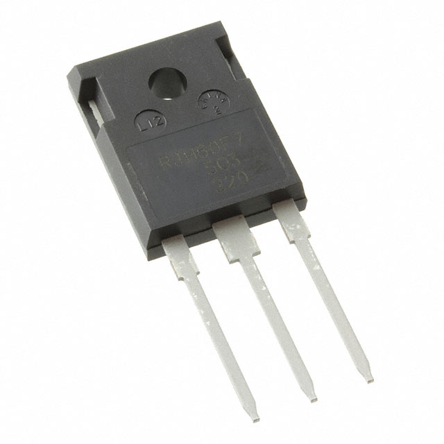
Outline
RENESAS Package code: PRSS0003ZH-A
(Package name: TO-247A)
C
4
1. Gate
2. Collector
3. Emitter
4. Collector
G
1 2
E
3
Absolute Maximum Ratings
(Tc = 25 C)
Item
Collector to emitter voltage
Gate to emitter voltage
Collector current
Tc = 25 C
Tc = 100 C
Collector peak current
Collector to emitter diode Tc = 25 C
Forward current
Tc = 100 C
Collector to emitter diode forward peak current
Collector dissipation
Junction to case thermal impedance (IGBT)
Junction to case thermal impedance (Diode)
Junction temperature
Storage temperature
Note:
Symbol
VCES
VGES
IC Note1
IC Note1
iC(peak) Note1
IDF
Ratings
650
30
100
50
180
40
Unit
V
V
A
A
A
A
IDF
iDF(peak) Note2
PC
j-c Note3
j-cd Note3
Tj Note4
Tstg
20
100
250
0.6
1.33
175
–55 to +150
A
A
W
C/W
C/W
°C
°C
Continuous heavy condition (e.g. high temperature/voltage/current or high variation of temperature) may affect a
reliability even if it are within the absolute maximum ratings. Please consider derating condition for appropriate
reliability in reference Renesas Semiconductor Reliability Handbook (Recommendation for Handling and Usage
of Semiconductor Devices) and individual reliability data.
R07DS1256EJ0110 Rev.1.10
Aug 31, 2018
Page 1 of 9
�RJH65T14DPQ-A0
Electrical Characteristics
(Tc = 25 C)
Item
Zero gate voltage collector current
Gate to emitter leak current
Gate to emitter cutoff voltage
Collector to emitter saturation
voltage
Symbol
ICES
IGES
VGE(off)
VCE(sat)
Min
4
Typ
1.45
Max
100
±1
7
1.75
Unit
A
A
V
V
Test Conditions
VCE = 650 V, VGE = 0 V
VGE = ±30 V, VCE = 0 V
VCE = 10 V, IC = 1 mA
IC = 50 A, VGE = 15 V Note5
Input capacitance
Output capacitance
Reveres transfer capacitance
Total gate charge
Gate to emitter charge
Gate to collector charge
Turn-on delay time
Rise time
Turn-off delay time
Fall time
Turn-on loss energy
Turn-off loss energy
Total switching energy
Turn-on delay time
Rise time
Turn-off delay time
Fall time
Turn-on loss energy
Turn-off loss energy
Total switching energy
Tail loss
Cies
Coes
Cres
Qg
Qge
Qgc
td(on)
tr
td(off)
tf
Eon
Eoff
Etotal
td(on)
tr
td(off)
tf
Eon
Eoff
Etotal
Etail
—
—
—
—
—
—
—
—
—
—
—
—
—
—
—
—
—
—
—
1750
69
34
80
15
35
38
30
125
115
1.3
1.2
2.5
38
30
130
135
1.45
1.45
2.90
560
—
—
—
—
—
—
—
—
—
—
—
—
—
—
—
—
—
—
—
pF
pF
pF
nC
nC
nC
ns
ns
ns
ns
mJ
mJ
mJ
ns
ns
ns
ns
mJ
mJ
mJ
J
VCE = 25 V
VGE = 0 V
f = 1 MHz
C-E diode forward voltage
C-E diode reverse recovery time
VECF
trr
1.2
250
1.6
V
ns
IF = 20 A Note5
IF = 20 A
diFdt = 300 As
VGE = 15 V
VCE = 300 V
IC = 50 A
VCC = 400 V
VGE = 15 V
IC = 50 A
Rg = 10
TC = 25 C
Inductive load
VCC = 400 V
VGE = 15 V
IC = 50 A
Rg = 10
TC = 150 C
Inductive load
VCC = 300 V, VGE = 20 V
IC = 50 A, Rg = 15
Tc = 125 C
Current resonance circuit
Notes: 1.
2.
3.
4.
Pulse width limited by safe operating area.
PW 5 s, duty cycle 1%
Value at Tc = 25 C
Please use this device in the thermal conditions which the junction temperature does not exceed 175 C.
Renesas IGBT Application Note is disclosed about reliability test and application condition up to 175 C.
5. Pulse test
R07DS1256EJ0110 Rev.1.10
Aug 31, 2018
Page 2 of 9
�RJH65T14DPQ-A0
Main Characteristics
Collector Dissipation vs.
Case Temperature
Maximum DC Collector Current vs.
Case Temperature
120
Collector Current IC (A)
Collector Dissipation PC (W)
300
200
100
80
60
40
20
0
0
0
25
50
75
100 125 150 175
0
50
75
100 125 150 175
Case Temperature Tc (C)
Maximum Safe Operation Area
Typical Transfer Characteristics
120
100
0
s
10
10
=1
Collector Current IC (A)
PW
0
s
1
0.1
0.01
1
Tc = 25 C
Single pulse Notes 6
VCE = 10 V
Pulse Test
90
60
150 C
Tc = 25 C
30
0
10
100
1000
0
Collector to Emitter Voltage VCE (V)
120
Pulse Test
2
Tc = 25 C
Pulse Test
2
Tc = 150 C
10 V
9.0 V
15 V
90
4
6
8
10
Typical Output Characteristics
Collector Current IC (A)
120
2
Gate to Emitter Voltage VGE (V)
Typical Output Characteristics
Collector Current IC (A)
25
Case Temperature Tc (C)
1000
Collector Current IC (A)
100
60
8.0 V
30
10 V
9.0 V
15 V
90
8.0 V
60
30
VGE = 7.0 V
VGE = 7.0 V
0
0
1
2
3
4
5
Collector to Emitter Voltage VCE (V)
0
0
1
2
3
4
5
Collector to Emitter Voltage VCE (V)
Notes: 6. This data is the designed value on Renesas’s measurement condition, Renesas recommends that operating
conditions are designed according to a document “Power MOSFET/IGBT Attention of Handling
Semiconductor Devices (R07ZZ0010)”.
R07DS1256EJ0110 Rev.1.10
Aug 31, 2018
Page 3 of 9
�RJH65T14DPQ-A0
Collector to Emitter Saturation Voltage
vs. Gate to Emitter Voltage (Typical)
Tc = 25 C
Pulse Test
4
IC = 100 A
50 A
25 A
3
2
1
0
4
8
12
16
20
IC = 100 A
4
Tc = 150 C
Pulse Test
50 A
25 A
3
2
1
0
4
8
12
16
20
Gate to Emitter Voltage VGE (V)
Gate to Emitter Cutoff Voltage
vs. Case Temperature (Typical)
Collector to Emitter Saturation Voltage
vs. Case Temperature (Typical)
8
IC = 10 mA
6
4
0
25
5
Gate to Emitter Voltage VGE (V)
10
2
Collector to Emitter Saturation Voltage
VCE(sat) (V)
5
1.0 mA
VCE = 10 V
Pulse Test
0
25
50
75
100 125 150
Case Temperature Tc (C)
R07DS1256EJ0110 Rev.1.10
Aug 31, 2018
Collector to Emitter Saturation Voltage
VCE(sat) (V)
Gate to Emitter Cutoff Voltage VGE(off) (V)
Collector to Emitter Saturation Voltage
VCE(sat) (V)
Collector to Emitter Saturation Voltage
vs. Gate to Emitter Voltage (Typical)
3.0
2.5
VGE = 15 V
Pulse Test
IC = 100 A
2.0
50 A
1.5
25 A
1.0
0.5
0
25
0
25
50
75
100 125 150
Case Temperature Tc (C)
Page 4 of 9
�RJH65T14DPQ-A0
Switching Characteristics (Typical) (1)
Switching Energy Losses E (mJ)
Switching Times t (ns)
1000
tf
td(off)
100
td(on)
tr
10
1
10
Switching Characteristics (Typical) (2)
VCC = 400 V, VGE = 15 V
Rg = 10 , Tc = 150 C
100
10
VCC = 400 V, VGE = 15 V
Rg = 10 , Tc = 150 C
Eoff
1
Eon
0.1
10
Collector Current IC (A)
(Inductive load)
Collector Current IC (A)
(Inductive load)
Switching Characteristics (Typical) (4)
Switching Characteristics (Typical) (3)
Switching Energy Losses E (mJ)
Switching Times t (ns)
1000
VCC = 400 V, VGE = 15 V
IC = 50 A, Tc = 150 C
tf
100
td(off)
td(on)
tr
10
1
10
100
10
VCC = 400 V, VGE = 15 V
IC = 50 A, Tc = 150 C
Eon
Eoff
1
1
Switching Energy Losses E (mJ)
Switching Times t (ns)
VCC = 400 V, VGE = 15 V
IC = 50 A, Rg = 10
td(off)
tf
td(on)
tr
10
1
25
50
75
100
125
Case Temperature Tc (C)
(Inductive load)
R07DS1256EJ0110 Rev.1.10
Aug 31, 2018
100
Switching Characteristics (Typical) (6)
Switching Characteristics (Typical) (5)
100
10
Gate Registance Rg ()
(Inductive load)
Gate Registance Rg ()
(Inductive load)
1000
100
150
10
VCC = 400 V, VGE = 15 V
IC = 50 A, Rg = 10
Eon
1
25
Eoff
50
75
100
125
150
Case Temperature Tc (C)
(Inductive load)
Page 5 of 9
�RJH65T14DPQ-A0
Typical Capacitance vs.
Collector to Emitter Voltage
Cies
1000
100
Coes
10
Cres
1
0
50
100
150
200
250
300
800
600
VCE
8
200
0
0
Tc = 150 C
400
25 C
200
0
40
60
80
Forward Current IF (A)
R07DS1256EJ0110 Rev.1.10
Aug 31, 2018
20
40
IC = 50 A
Ta = 25 C
60
80
0
100
100
100
Forward Current IF (A)
Reverse Recovery Time trr (ns)
VCC = 300 V
diF/dt = 300 As
20
4
VCC = 480 V
300 V
120 V
Forward Current vs. Forward Voltage (Typical)
1000
0
12
Gate Charge Qg (nC)
Reverse Recovery Time vs.
Forward Current (Typical)
600
VCC = 480 V
300 V
120 V
400
Collector to Emitter Voltage VCE (V)
800
16
VGE
Gate to Emitter Voltage VGE (V)
VGE = 0 V, Tc = 25 C
f = 1 MHz
Collector to Emitter Voltage VCE (V)
Capacitance C (pF)
10000
Dynamic Input Characteristics (Typical)
Tc = 25 C
80
150 C
60
40
20
0
VCE = 0 V
Pulse Test
0
1
2
3
4
C-E Diode Forward Voltage VCEF (V)
Page 6 of 9
�Normalized Transient Thermal Impedance s (t)
RJH65T14DPQ-A0
Normalized Transient Thermal Impedance vs. Pulse Width (IGBT)
10
1
D=1
0.5
j – c(t) = s (t) • j – c
j – c = 0.60C/W, Tc = 25C
0.2
0.1
0 .1
0 .0 5
PDM
0.02
0.01
1 shot pulse
0.01
10
100
D=
PW
T
PW
T
1m
10 m
Pulse Width
100 m
1
10
PW (s)
Normalized Transient Thermal Impedance s (t)
Normalized Transient Thermal Impedance vs. Pulse Width (Diode)
10
1
D=1
0.5
0.2
0.1
0.05
j – c(t) = s (t) • j – c
j – c = 1.33C/W, Tc = 25C
0.1
PDM
0.02
0.01
1 shot pulse
0.01
10
R07DS1256EJ0110 Rev.1.10
Aug 31, 2018
100
D=
PW
T
PW
T
1m
10 m
Pulse Width
100 m
1
10
PW (s)
Page 7 of 9
�RJH65T14DPQ-A0
Waveform
Switching Time Test Circuit
VGE
Diode clamp
90%
10%
L
IC
90%
D.U.T
90%
VCC
Rg
10%
td(off)
Diode Reverse Recovery Time Test Circuit
10%
tf
td(on)
tr
Waveform
VCC
IF
D.U.T
IF
diF/dt
L
trr
0
Irr
Rg
R07DS1256EJ0110 Rev.1.10
Aug 31, 2018
0.5 Irr
0.9 Irr
Page 8 of 9
�RJH65T14DPQ-A0
Package Dimensions
JEDEC Package Code
RENESAS Code
Previous Code
MASS (Typ) [g]
TO-247A
PRSS0003ZH-A
—
6.14
Unit: mm
15.94±0.19
5.02±0.19
3.6±0.1
21.13±0.33
17.86
6.15
Pin No. 4
13.26
4.5 max.
20.19±0.38
2.41
Pin No. 1
2
3
1.27 +− 0.13
0.20
3.12
2.10 +− 0.31
0.20
0.71 +− 0.10
0.16
5.45 5.45
+ 0.26
− 0.25
© 2018 Renesas Electronics Corporation. All rights reserved.
Ordering Information
Orderable Part Number
RJH65T14DPQ-A0#T0
R07DS1256EJ0110 Rev.1.10
Aug 31, 2018
Quantity
240 pcs
Shipping Container
Box (Tube)
Page 9 of 9
�Notice
1.
Descriptions of circuits, software and other related information in this document are provided only to illustrate the operation of semiconductor products and application examples. You are fully responsible for
the incorporation or any other use of the circuits, software, and information in the design of your product or system. Renesas Electronics disclaims any and all liability for any losses and damages incurred by
you or third parties arising from the use of these circuits, software, or information.
2.
Renesas Electronics hereby expressly disclaims any warranties against and liability for infringement or any other claims involving patents, copyrights, or other intellectual property rights of third parties, by or
arising from the use of Renesas Electronics products or technical information described in this document, including but not limited to, the product data, drawings, charts, programs, algorithms, and application
examples.
3.
No license, express, implied or otherwise, is granted hereby under any patents, copyrights or other intellectual property rights of Renesas Electronics or others.
4.
You shall not alter, modify, copy, or reverse engineer any Renesas Electronics product, whether in whole or in part. Renesas Electronics disclaims any and all liability for any losses or damages incurred by
5.
Renesas Electronics products are classified according to the following two quality grades: “Standard” and “High Quality”. The intended applications for each Renesas Electronics product depends on the
you or third parties arising from such alteration, modification, copying or reverse engineering.
product’s quality grade, as indicated below.
"Standard":
Computers; office equipment; communications equipment; test and measurement equipment; audio and visual equipment; home electronic appliances; machine tools; personal electronic
equipment; industrial robots; etc.
"High Quality": Transportation equipment (automobiles, trains, ships, etc.); traffic control (traffic lights); large-scale communication equipment; key financial terminal systems; safety control equipment; etc.
Unless expressly designated as a high reliability product or a product for harsh environments in a Renesas Electronics data sheet or other Renesas Electronics document, Renesas Electronics products are
not intended or authorized for use in products or systems that may pose a direct threat to human life or bodily injury (artificial life support devices or systems; surgical implantations; etc.), or may cause
serious property damage (space system; undersea repeaters; nuclear power control systems; aircraft control systems; key plant systems; military equipment; etc.). Renesas Electronics disclaims any and all
liability for any damages or losses incurred by you or any third parties arising from the use of any Renesas Electronics product that is inconsistent with any Renesas Electronics data sheet, user’s manual or
other Renesas Electronics document.
6.
When using Renesas Electronics products, refer to the latest product information (data sheets, user’s manuals, application notes, “General Notes for Handling and Using Semiconductor Devices” in the
reliability handbook, etc.), and ensure that usage conditions are within the ranges specified by Renesas Electronics with respect to maximum ratings, operating power supply voltage range, heat dissipation
characteristics, installation, etc. Renesas Electronics disclaims any and all liability for any malfunctions, failure or accident arising out of the use of Renesas Electronics products outside of such specified
ranges.
7.
Although Renesas Electronics endeavors to improve the quality and reliability of Renesas Electronics products, semiconductor products have specific characteristics, such as the occurrence of failure at a
certain rate and malfunctions under certain use conditions. Unless designated as a high reliability product or a product for harsh environments in a Renesas Electronics data sheet or other Renesas
Electronics document, Renesas Electronics products are not subject to radiation resistance design. You are responsible for implementing safety measures to guard against the possibility of bodily injury, injury
or damage caused by fire, and/or danger to the public in the event of a failure or malfunction of Renesas Electronics products, such as safety design for hardware and software, including but not limited to
redundancy, fire control and malfunction prevention, appropriate treatment for aging degradation or any other appropriate measures. Because the evaluation of microcomputer software alone is very difficult
and impractical, you are responsible for evaluating the safety of the final products or systems manufactured by you.
8.
Please contact a Renesas Electronics sales office for details as to environmental matters such as the environmental compatibility of each Renesas Electronics product. You are responsible for carefully and
sufficiently investigating applicable laws and regulations that regulate the inclusion or use of controlled substances, including without limitation, the EU RoHS Directive, and using Renesas Electronics
products in compliance with all these applicable laws and regulations. Renesas Electronics disclaims any and all liability for damages or losses occurring as a result of your noncompliance with applicable
laws and regulations.
9.
Renesas Electronics products and technologies shall not be used for or incorporated into any products or systems whose manufacture, use, or sale is prohibited under any applicable domestic or foreign laws
or regulations. You shall comply with any applicable export control laws and regulations promulgated and administered by the governments of any countries asserting jurisdiction over the parties or
transactions.
10. It is the responsibility of the buyer or distributor of Renesas Electronics products, or any other party who distributes, disposes of, or otherwise sells or transfers the product to a third party, to notify such third
party in advance of the contents and conditions set forth in this document.
11. This document shall not be reprinted, reproduced or duplicated in any form, in whole or in part, without prior written consent of Renesas Electronics.
12. Please contact a Renesas Electronics sales office if you have any questions regarding the information contained in this document or Renesas Electronics products.
(Note 1)
“Renesas Electronics” as used in this document means Renesas Electronics Corporation and also includes its directly or indirectly controlled subsidiaries.
(Note 2)
“Renesas Electronics product(s)” means any product developed or manufactured by or for Renesas Electronics.
(Rev.4.0-1 November 2017)
http://www.renesas.com
SALES OFFICES
Refer to "http://www.renesas.com/" for the latest and detailed information.
Renesas Electronics America Inc.
1001 Murphy Ranch Road, Milpitas, CA 95035, U.S.A.
Tel: +1-408-432-8888, Fax: +1-408-434-5351
Renesas Electronics Canada Limited
9251 Yonge Street, Suite 8309 Richmond Hill, Ontario Canada L4C 9T3
Tel: +1-905-237-2004
Renesas Electronics Europe Limited
Dukes Meadow, Millboard Road, Bourne End, Buckinghamshire, SL8 5FH, U.K
Tel: +44-1628-651-700, Fax: +44-1628-651-804
Renesas Electronics Europe GmbH
Arcadiastrasse 10, 40472 Düsseldorf, Germany
Tel: +49-211-6503-0, Fax: +49-211-6503-1327
Renesas Electronics (China) Co., Ltd.
Room 1709 Quantum Plaza, No.27 ZhichunLu, Haidian District, Beijing, 100191 P. R. China
Tel: +86-10-8235-1155, Fax: +86-10-8235-7679
Renesas Electronics (Shanghai) Co., Ltd.
Unit 301, Tower A, Central Towers, 555 Langao Road, Putuo District, Shanghai, 200333 P. R. China
Tel: +86-21-2226-0888, Fax: +86-21-2226-0999
Renesas Electronics Hong Kong Limited
Unit 1601-1611, 16/F., Tower 2, Grand Century Place, 193 Prince Edward Road West, Mongkok, Kowloon, Hong Kong
Tel: +852-2265-6688, Fax: +852 2886-9022
Renesas Electronics Taiwan Co., Ltd.
13F, No. 363, Fu Shing North Road, Taipei 10543, Taiwan
Tel: +886-2-8175-9600, Fax: +886 2-8175-9670
Renesas Electronics Singapore Pte. Ltd.
80 Bendemeer Road, Unit #06-02 Hyflux Innovation Centre, Singapore 339949
Tel: +65-6213-0200, Fax: +65-6213-0300
Renesas Electronics Malaysia Sdn.Bhd.
Unit 1207, Block B, Menara Amcorp, Amcorp Trade Centre, No. 18, Jln Persiaran Barat, 46050 Petaling Jaya, Selangor Darul Ehsan, Malaysia
Tel: +60-3-7955-9390, Fax: +60-3-7955-9510
Renesas Electronics India Pvt. Ltd.
No.777C, 100 Feet Road, HAL 2nd Stage, Indiranagar, Bangalore 560 038, India
Tel: +91-80-67208700, Fax: +91-80-67208777
Renesas Electronics Korea Co., Ltd.
17F, KAMCO Yangjae Tower, 262, Gangnam-daero, Gangnam-gu, Seoul, 06265 Korea
Tel: +82-2-558-3737, Fax: +82-2-558-5338
© 2018 Renesas Electronics Corporation. All rights reserved.
Colophon 7.0
�