STD65N55F3
Datasheet
Automotive-grade N-channel 55 V, 6.5 mΩ typ., 80 A STripFET F3
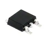
Power MOSFET in a DPAK package
Features
TAB
2 3
1
DPAK
•
•
Type
VDS
RDS(on) max.
ID
PTOT
STD65N55F3
55 V
8.5 mΩ
80 A
110 W
AEC-Q101 qualified
100% avalanche tested
D(2, TAB)
Applications
•
Switching applications
G(1)
Description
S(3)
AM01475v1_noZen
This device is an N-channel Power MOSFET developed using STripFET™ F3
technology. It is designed to minimize on-resistance and gate charge to provide
superior switching performance.
Product status
STD65N55F3
Product summary
Order code
STD65N55F3
Marking
65N55F3
Package
DPAK
Packing
Tape and reel
DS5128 - Rev 5 - January 2019
For further information contact your local STMicroelectronics sales office.
www.st.com
�STD65N55F3
Electrical ratings
1
Electrical ratings
Table 1. Absolute maximum ratings
Symbol
Parameter
Value
Unit
VDS
Drain-source voltage
55
V
VGS
Gate-source voltage
±20
V
Drain current (continuous) at TC = 25 °C
80
A
Drain current (continuous) at TC = 100 °C
56
A
IDM
Drain current (pulsed)
320
A
PTOT
Total power dissipation at TC = 25 °C
110
W
Peak diode recovery
11
V/ns
390
mJ
-55 to 175
°C
Value
Unit
ID
(1)
dv/dt(2)
(3)
EAS
Tj
Tstg
Single pulse avalanche energy
Operating junction temperature range
Storage temperature range
1. Pulse width is limited by safe operating area.
2. ISD ≤ 65A, di/dt ≤ 300 A/μs, VDD ≤ V(BR)DSS, Tj ≤ Tjmax
3. Starting Tj = 25°C, ID = 32 A, VDD = 25 V
Table 2. Thermal resistance
Symbol
Parameter
Rthj-case
Thermal resistance junction-case
1.36
°C/W
Rthj-pcb(1)
Thermal resistance junction-pcb
50
°C/W
1. When mounted on an 1- inch² FR-4 board, 2oz Cu.
DS5128 - Rev 5
page 2/17
�STD65N55F3
Electrical characteristics
2
Electrical characteristics
TC = 25 °C unless otherwise specified
Table 3. Static characteristics
Symbol
V(BR)DSS
Parameter
Drain-source breakdown
voltage
Test conditions
Min.
VGS = 0 V, ID = 250 µA
Typ.
55
Zero gate voltage drain
current
IGSS
Gate-body leakage current
VGS = ±20 V, VDS = 0 V
VGS(th)
Gate threshold voltage
VDS = VGS, ID = 250 µA
RDS(on)
Static drain-source onresistance
VGS = 10 V, ID = 32 A
VGS = 0 V, VDS = 55 V, TC = 125
Unit
V
VGS = 0 V, VDS = 55 V
IDSS
Max.
10
µA
100
µA
±200
nA
4
V
6.5
8.5
mΩ
Min.
Typ.
Max.
Unit
-
2200
pF
-
500
pF
-
25
pF
°C(1)
2
1. Defined by design, not subject to production test.
Table 4. Dynamic characteristics
Symbol
Parameter
Test conditions
Ciss
Input capacitance
Coss
Output capacitance
Crss
Reverse transfer capacitance
Qg
Total gate charge
VDD = 27 V, ID = 65 A,
-
33.5
Qgs
Gate-source charge
VGS = 0 to 10 V
-
12.5
nC
Qgd
Gate-drain charge
(see Figure 13. Test circuit for gate charge
behavior)
-
9.5
nC
Min.
Typ.
Max.
Unit
VDS = 25 V, f = 1 MHz, VGS = 0 V
45
nC
Table 5. Switching times
Symbol
td(on)
tr
td(off)
tf
DS5128 - Rev 5
Parameter
Test conditions
Turn-on delay time
VDD= 27 V, ID = 32 A,
-
20
-
ns
Rise time
RG = 4.7 Ω, VGS = 10 V
-
50
-
ns
Turn-off delay time
(see Figure 12. Test circuit for resistive load
switching times and Figure 17. Switching time
waveform)
-
35
-
ns
-
11.5
-
ns
Fall time
page 3/17
�STD65N55F3
Electrical characteristics
Table 6. Source-drain diode
Symbol
ISD
ISDM(1)
VSD
Parameter
Test conditions
Min.
Typ.
Max.
Unit
Source-drain current
80
A
Source-drain current (pulsed)
320
A
1.5
V
Forward on voltage
ISD = 65 A, VGS = 0 V
-
trr
Reverse recovery time
ISD = 65 A, di/dt = 100 A/μs,
-
47
ns
Qrr
Reverse recovery charge
VDD = 25 V, Tj = 150 °C
-
87
nC
Reverse recovery current
(see Figure 14. Test circuit for inductive load
switching and diode recovery times)
-
3.7
A
IRRM
1. Pulsed: pulse duration = 300 μs, duty cycle 1.5%
DS5128 - Rev 5
page 4/17
�STD65N55F3
Electrical characteristics (curves)
2.1
DS5128 - Rev 5
Electrical characteristics (curves)
Figure 1. Safe operating area
Figure 2. Thermal impedance
Figure 3. Output characteristics
Figure 4. Transfer characteristics
page 5/17
�STD65N55F3
Electrical characteristics (curves)
Figure 5. Normalized V(BR)DSS vs temperature
V(BR)DSS
(norm.)
Figure 6. Static drain-source on-resistance
HV36510
ID = 250 μA
1.10
1.05
1.00
0.95
0.90
0.85
-100
-50
0
50
100
150
TJ (°C)
Figure 7. Gate charge vs gate-source voltage
Figure 8. Capacitance variations
V
Figure 9. Normalized gate threshold voltage vs
temperature
-100
DS5128 - Rev 5
Figure 10. Normalized on-resistance vs temperature
0
-100
page 6/17
�STD65N55F3
Electrical characteristics (curves)
Figure 11. Source-drain diode forward characteristics
DS5128 - Rev 5
page 7/17
�STD65N55F3
Test circuits
3
Test circuits
Figure 12. Test circuit for resistive load switching times
Figure 13. Test circuit for gate charge behavior
VDD
12 V
2200
+ μF
3.3
μF
VDD
VD
VGS
1 kΩ
100 nF
RL
IG= CONST
VGS
RG
47 kΩ
+
pulse width
D.U.T.
2.7 kΩ
2200
μF
pulse width
D.U.T.
100 Ω
VG
47 kΩ
1 kΩ
AM01469v1
AM01468v1
Figure 14. Test circuit for inductive load switching and
diode recovery times
D
G
A
D.U.T.
S
25 Ω
A
L
A
B
B
3.3
µF
D
G
+
VD
100 µH
fast
diode
B
Figure 15. Unclamped inductive load test circuit
RG
1000
+ µF
2200
+ µF
VDD
3.3
µF
VDD
ID
D.U.T.
S
D.U.T.
Vi
_
pulse width
AM01471v1
AM01470v1
Figure 17. Switching time waveform
Figure 16. Unclamped inductive waveform
ton
V(BR)DSS
td(on)
VD
toff
td(off)
tr
tf
90%
90%
IDM
VDD
10%
0
ID
VDD
AM01472v1
VGS
0
VDS
10%
90%
10%
AM01473v1
DS5128 - Rev 5
page 8/17
�STD65N55F3
Package information
4
Package information
In order to meet environmental requirements, ST offers these devices in different grades of ECOPACK®
packages, depending on their level of environmental compliance. ECOPACK® specifications, grade definitions
and product status are available at: www.st.com. ECOPACK® is an ST trademark.
DS5128 - Rev 5
page 9/17
�STD65N55F3
DPAK (TO-252) type A2 package information
4.1
DPAK (TO-252) type A2 package information
Figure 18. DPAK (TO-252) type A2 package outline
0068772_type-A2_rev26
DS5128 - Rev 5
page 10/17
�STD65N55F3
DPAK (TO-252) type A2 package information
Table 7. DPAK (TO-252) type A2 mechanical data
Dim.
mm
Min.
Max.
A
2.20
2.40
A1
0.90
1.10
A2
0.03
0.23
b
0.64
0.90
b4
5.20
5.40
c
0.45
0.60
c2
0.48
0.60
D
6.00
6.20
D1
4.95
E
6.40
E1
5.10
5.20
5.30
e
2.159
2.286
2.413
e1
4.445
4.572
4.699
H
9.35
10.10
L
1.00
1.50
L1
2.60
2.80
3.00
L2
0.65
0.80
0.95
L4
0.60
R
V2
DS5128 - Rev 5
Typ.
5.10
5.25
6.60
1.00
0.20
0°
8°
page 11/17
�STD65N55F3
DPAK (TO-252) type A2 package information
Figure 19. DPAK (TO-252) recommended footprint (dimensions are in mm)
FP_0068772_rev26
DS5128 - Rev 5
page 12/17
�STD65N55F3
DPAK (TO-252) packing information
4.2
DPAK (TO-252) packing information
Figure 20. DPAK (TO-252) tape outline
10 pitches cumulative
tolerance on tape +/- 0.2 mm
T
P0
Top cover
tape
P2
D
E
F
B1
K0
For machine ref. only
including draft and
radii concentric around B0
W
B0
A0
P1
D1
User direction of feed
R
Bending radius
User direction of feed
AM08852v1
DS5128 - Rev 5
page 13/17
�STD65N55F3
DPAK (TO-252) packing information
Figure 21. DPAK (TO-252) reel outline
T
40mm min.
access hole
at slot location
B
D
C
N
A
G measured
at hub
Tape slot
in core for
tape start
2.5mm min.width
Full radius
AM06038v1
Table 8. DPAK (TO-252) tape and reel mechanical data
Tape
Dim.
mm
mm
Dim.
Min.
Max.
A0
6.8
7
A
B0
10.4
10.6
B
1.5
12.1
C
12.8
1.6
D
20.2
G
16.4
50
B1
DS5128 - Rev 5
Reel
Min.
Max.
330
13.2
D
1.5
D1
1.5
E
1.65
1.85
N
F
7.4
7.6
T
K0
2.55
2.75
P0
3.9
4.1
Base qty.
2500
P1
7.9
8.1
Bulk qty.
2500
P2
1.9
2.1
R
40
T
0.25
0.35
W
15.7
16.3
18.4
22.4
page 14/17
�STD65N55F3
Revision history
Table 9. Document revision history
Date
Version
Changes
08-Feb-2007
1
First release.
22-Feb-2007
2
Description has been changed
11-May-2007
3
Improved current values
Updated information on cover page.
13-Feb-2018
4
Updated Section 1 Electrical ratings
and Section 2 Electrical characteristics.
Updated Section 4.1 DPAK (TO-252) type A2 package information.
Minor text changes.
17-Jan-2019
DS5128 - Rev 5
5
Updated Section 4.1 DPAK (TO-252) type A2 package information.
Minor text changes.
page 15/17
�STD65N55F3
Contents
Contents
1
Electrical ratings . . . . . . . . . . . . . . . . . . . . . . . . . . . . . . . . . . . . . . . . . . . . . . . . . . . . . . . . . . . . . . . . . .2
2
Electrical characteristics. . . . . . . . . . . . . . . . . . . . . . . . . . . . . . . . . . . . . . . . . . . . . . . . . . . . . . . . . . . 3
2.1
Electrical characteristics (curves) . . . . . . . . . . . . . . . . . . . . . . . . . . . . . . . . . . . . . . . . . . . . . . . . . 5
3
Test circuits . . . . . . . . . . . . . . . . . . . . . . . . . . . . . . . . . . . . . . . . . . . . . . . . . . . . . . . . . . . . . . . . . . . . . . .8
4
Package information. . . . . . . . . . . . . . . . . . . . . . . . . . . . . . . . . . . . . . . . . . . . . . . . . . . . . . . . . . . . . . .9
4.1
DPAK (TO-252) type A2 package information . . . . . . . . . . . . . . . . . . . . . . . . . . . . . . . . . . . . . . . 9
4.2
DPAK (TO-252) packing information. . . . . . . . . . . . . . . . . . . . . . . . . . . . . . . . . . . . . . . . . . . . . . 12
Revision history . . . . . . . . . . . . . . . . . . . . . . . . . . . . . . . . . . . . . . . . . . . . . . . . . . . . . . . . . . . . . . . . . . . . . . .15
DS5128 - Rev 5
page 16/17
�STD65N55F3
IMPORTANT NOTICE – PLEASE READ CAREFULLY
STMicroelectronics NV and its subsidiaries (“ST”) reserve the right to make changes, corrections, enhancements, modifications, and improvements to ST
products and/or to this document at any time without notice. Purchasers should obtain the latest relevant information on ST products before placing orders. ST
products are sold pursuant to ST’s terms and conditions of sale in place at the time of order acknowledgement.
Purchasers are solely responsible for the choice, selection, and use of ST products and ST assumes no liability for application assistance or the design of
Purchasers’ products.
No license, express or implied, to any intellectual property right is granted by ST herein.
Resale of ST products with provisions different from the information set forth herein shall void any warranty granted by ST for such product.
ST and the ST logo are trademarks of ST. All other product or service names are the property of their respective owners.
Information in this document supersedes and replaces information previously supplied in any prior versions of this document.
© 2019 STMicroelectronics – All rights reserved
DS5128 - Rev 5
page 17/17
�
很抱歉,暂时无法提供与“STD65N55F3”相匹配的价格&库存,您可以联系我们找货
免费人工找货- 国内价格 香港价格
- 2500+8.607612500+1.10969
- 5000+8.086395000+1.04249
- 7500+8.022727500+1.03429
- 国内价格
- 1+9.03096
- 10+7.61703
- 30+6.32189
- 100+6.21108
- 国内价格
- 1+23.35511
- 10+15.35231
- 13+8.73775
- 36+8.32944
- 2500+8.08446