STSPIN820
Advanced 256 microsteps integrated motor driver with
step-clock and direction interface
Datasheet - production data
Applications
3D printers
Medical equipment
Industrial 2D printers
Textile and sewing machines
CCTV, security and dome cameras
ATM and cash handling machines
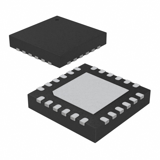
QFN 4 x 4 - 24 lead
Office and home automation
POS
Robotics
Features
Operating voltage from 7 to 45 V
Description
Maximum output current 1.5 Arms
The STSPIN820 is a stepper motor driver which
integrates, in a small QFN 4 x 4 mm package,
both control logic and a low RDSon power stage.
RDSon HS + LS = 1 Ω typ.
Microstepping up to 1/256th of step
Current control with programmable OFF time
Current sensing based on external shunt
resistor
Full protection set
Non-dissipative overcurrent protection
Short-circuit protection
Undervoltage lockout
The integrated controller implements a PWM
current control with fixed OFF time and a
microstepping resolution up to 1/256th of the step.
The device can be forced into a low consumption
state.
The device offers a complete set of protection
features including overcurrent, overtemperature
and short-circuit protection.
Thermal shutdown
Standby low consumption
December 2017
This is information on a product in full production.
DocID031065 Rev 2
1/29
www.st.com
�Contents
STSPIN820
Contents
1
Block diagram . . . . . . . . . . . . . . . . . . . . . . . . . . . . . . . . . . . . . . . . . . . . . . 5
2
Electrical data . . . . . . . . . . . . . . . . . . . . . . . . . . . . . . . . . . . . . . . . . . . . . . 6
2.1
Absolute maximum ratings . . . . . . . . . . . . . . . . . . . . . . . . . . . . . . . . . . . . . 6
2.2
Recommended operating conditions . . . . . . . . . . . . . . . . . . . . . . . . . . . . . 6
2.3
Thermal data . . . . . . . . . . . . . . . . . . . . . . . . . . . . . . . . . . . . . . . . . . . . . . . 6
2.4
ESD protection ratings . . . . . . . . . . . . . . . . . . . . . . . . . . . . . . . . . . . . . . . . 7
3
Electrical characteristics . . . . . . . . . . . . . . . . . . . . . . . . . . . . . . . . . . . . . 8
4
Pin connection . . . . . . . . . . . . . . . . . . . . . . . . . . . . . . . . . . . . . . . . . . . . . 10
5
Functional description . . . . . . . . . . . . . . . . . . . . . . . . . . . . . . . . . . . . . . 12
5.1
Power supply and standby . . . . . . . . . . . . . . . . . . . . . . . . . . . . . . . . . . . . 12
5.2
Microstepping sequencer . . . . . . . . . . . . . . . . . . . . . . . . . . . . . . . . . . . . . 13
5.3
PWM current control . . . . . . . . . . . . . . . . . . . . . . . . . . . . . . . . . . . . . . . . . 16
5.4
Overcurrent and short-circuit protections . . . . . . . . . . . . . . . . . . . . . . . . . 19
5.5
Thermal shutdown . . . . . . . . . . . . . . . . . . . . . . . . . . . . . . . . . . . . . . . . . . 22
5.6
ESD protection strategy . . . . . . . . . . . . . . . . . . . . . . . . . . . . . . . . . . . . . . 23
6
Typical applications . . . . . . . . . . . . . . . . . . . . . . . . . . . . . . . . . . . . . . . . 24
7
Layout recommendations . . . . . . . . . . . . . . . . . . . . . . . . . . . . . . . . . . . . 25
8
Package information . . . . . . . . . . . . . . . . . . . . . . . . . . . . . . . . . . . . . . . . 26
8.1
TFQFPN 4 x 4 x 1.05- 24L package information . . . . . . . . . . . . . . . . . . . 26
9
Ordering information . . . . . . . . . . . . . . . . . . . . . . . . . . . . . . . . . . . . . . . 28
10
Revision history . . . . . . . . . . . . . . . . . . . . . . . . . . . . . . . . . . . . . . . . . . . 28
2/29
DocID031065 Rev 2
�STSPIN820
List of tables
List of tables
Table 1.
Table 2.
Table 3.
Table 4.
Table 5.
Table 6.
Table 7.
Table 8.
Table 9.
Table 10.
Table 11.
Table 12.
Table 13.
Table 14.
Table 15.
Absolute maximum ratings . . . . . . . . . . . . . . . . . . . . . . . . . . . . . . . . . . . . . . . . . . . . . . . . . . 6
Recommended operating conditions . . . . . . . . . . . . . . . . . . . . . . . . . . . . . . . . . . . . . . . . . . 6
Thermal data. . . . . . . . . . . . . . . . . . . . . . . . . . . . . . . . . . . . . . . . . . . . . . . . . . . . . . . . . . . . . 6
ESD protection ratings . . . . . . . . . . . . . . . . . . . . . . . . . . . . . . . . . . . . . . . . . . . . . . . . . . . . . 7
Electrical characteristics . . . . . . . . . . . . . . . . . . . . . . . . . . . . . . . . . . . . . . . . . . . . . . . . . . . . 8
Pin description . . . . . . . . . . . . . . . . . . . . . . . . . . . . . . . . . . . . . . . . . . . . . . . . . . . . . . . . . . 10
Step mode selection through MODEx inputs . . . . . . . . . . . . . . . . . . . . . . . . . . . . . . . . . . . 13
Target reference and current direction according to sequencer value
(full-step mode) . . . . . . . . . . . . . . . . . . . . . . . . . . . . . . . . . . . . . . . . . . . . . . . . . . . . . . . . . . 14
Target reference and current direction according to sequencer value
(not full-step mode) . . . . . . . . . . . . . . . . . . . . . . . . . . . . . . . . . . . . . . . . . . . . . . . . . . . . . . . 14
Example . . . . . . . . . . . . . . . . . . . . . . . . . . . . . . . . . . . . . . . . . . . . . . . . . . . . . . . . . . . . . . . 15
ON, slow decay and fast decay states . . . . . . . . . . . . . . . . . . . . . . . . . . . . . . . . . . . . . . . . 16
Typical application values . . . . . . . . . . . . . . . . . . . . . . . . . . . . . . . . . . . . . . . . . . . . . . . . . . 24
TFQFPN 4 x 4 x 1.05 - 24L package mechanical data . . . . . . . . . . . . . . . . . . . . . . . . . . . . 27
Device summary . . . . . . . . . . . . . . . . . . . . . . . . . . . . . . . . . . . . . . . . . . . . . . . . . . . . . . . . . 28
Document revision history . . . . . . . . . . . . . . . . . . . . . . . . . . . . . . . . . . . . . . . . . . . . . . . . . 28
DocID031065 Rev 2
3/29
29
�List of figures
STSPIN820
List of figures
Figure 1.
Figure 2.
Figure 3.
Figure 4.
Figure 5.
Figure 6.
Figure 7.
Figure 8.
Figure 9.
Figure 10.
Figure 11.
Figure 12.
Figure 13.
Figure 14.
Figure 15.
Figure 16.
4/29
Block diagram . . . . . . . . . . . . . . . . . . . . . . . . . . . . . . . . . . . . . . . . . . . . . . . . . . . . . . . . . . . . 5
Pin connection (top view) . . . . . . . . . . . . . . . . . . . . . . . . . . . . . . . . . . . . . . . . . . . . . . . . . . 10
UVLO protection management . . . . . . . . . . . . . . . . . . . . . . . . . . . . . . . . . . . . . . . . . . . . . . 12
MODEx, STCK and DIR timing diagram . . . . . . . . . . . . . . . . . . . . . . . . . . . . . . . . . . . . . . . 13
PWM current control sequence in mixed decay (DECAY = '0') . . . . . . . . . . . . . . . . . . . . . 17
OFF time regulation circuit . . . . . . . . . . . . . . . . . . . . . . . . . . . . . . . . . . . . . . . . . . . . . . . . . 18
OFF time vs ROFF value . . . . . . . . . . . . . . . . . . . . . . . . . . . . . . . . . . . . . . . . . . . . . . . . . . . 18
Overcurrent and short-circuit protections management . . . . . . . . . . . . . . . . . . . . . . . . . . . 19
Disable time versus REN and CEN values (VDD = 3.3 V) . . . . . . . . . . . . . . . . . . . . . . . . . . 20
Overcurrent threshold versus temperature normalized at 25 °C . . . . . . . . . . . . . . . . . . . . 21
Thermal shutdown management . . . . . . . . . . . . . . . . . . . . . . . . . . . . . . . . . . . . . . . . . . . . 22
ESD protection strategy . . . . . . . . . . . . . . . . . . . . . . . . . . . . . . . . . . . . . . . . . . . . . . . . . . . 23
Typical application schematic . . . . . . . . . . . . . . . . . . . . . . . . . . . . . . . . . . . . . . . . . . . . . . . 24
PCB layout example (top layer) . . . . . . . . . . . . . . . . . . . . . . . . . . . . . . . . . . . . . . . . . . . . . 25
TFQFPN 4 x 4 x 1.05- 24L package outline . . . . . . . . . . . . . . . . . . . . . . . . . . . . . . . . . . . . 26
TFQFPN 4 x 4 x 1.05 - 24L suggested footprint . . . . . . . . . . . . . . . . . . . . . . . . . . . . . . . . . 27
DocID031065 Rev 2
�STSPIN820
1
Block diagram
Block diagram
Figure 1. Block diagram
74
67-0
075
74
45#:=3&4&5
%"$
74
065"�
0$=4$
&/= '"6-5
4&/4&"�
7SFMFBTF
�
�
�
065"�
$0/530-0(*$
45$,
�
0$=4$
�
4&/4&"�
%*3
74
.0%&�
4/4"
%"$
.0%&�
.0%&�
0$=4$
%&$":
4UFQQFS
NPUPS
065#�
4&/4&#�
�
50''
�
0TDJMMBUPS
0$=4$
065#�
4&/4&#�
4/4#
(/%
3&'
".������
DocID031065 Rev 2
5/29
29
�Electrical data
STSPIN820
2
Electrical data
2.1
Absolute maximum ratings
Table 1. Absolute maximum ratings
Symbol
Parameter
Test condition
Value
Unit
VS
Supply voltage
-
-0.3 to 48
V
VIN
Logic input voltage
-
-0.3 to 5.5
V
VOUT,diff Differential voltage between VS, OUTx1, OUTx2 and SENSEx pins
-
up to 48
V
VSENSE
Sense pins voltage
-
-2 to 2
V
Reference voltage input
-
-0.3 to 2
V
-
1.5
Arms
VREF
IOUT,RMS Continuous power stage output current (each full-bridge)
Tj
Junction temperature
-
-40 to 150
°C
TSTG
Storage temperature
-
-55 to 150
°C
2.2
Recommended operating conditions
Table 2. Recommended operating conditions
Symbol
Parameter
Min.
Typ.
Max.
Unit
VS
Supply voltage
7
-
45
V
VIN
Logic input voltage
-
-
5
V
VSENSE
Sense pins voltage
-1
-
+1
V
Reference voltage input
0.1
-
1
V
VREF
2.3
Thermal data
Table 3. Thermal data
Symbol
RthJA
Parameter
Conditions
(1)
Value
Unit
36.5
°C/W
Junction to ambient thermal resistance
Natural convection, according to JESD51-2A
RthJCtop
Junction to case thermal resistance
(top side)
Cold plate on top package, according to
JESD51-12(1)
27.6
°C/W
RthJCbot
Junction to case thermal resistance
(bottom side)
Cold plate on exposed pad, according to
JESD51-12(1)
5.9
°C/W
RthJB
Junction to board thermal resistance
according to JESD51-8(1)
JT
JB
Junction to top characterization
Junction to board characterization
13.6
°C/W
According to
JESD51-2A(1)
1
°C/W
According to
JESD51-2A(1)
13.7
°C/W
1. Simulated on a 76.2 x 114.3 x 1.6 mm, with vias underneath the component, the 2s2p board as per the standard JEDEC
(JESD51-7) in natural convection.
6/29
DocID031065 Rev 2
�STSPIN820
2.4
Electrical data
ESD protection ratings
Table 4. ESD protection ratings
Symbol
HBM
CDM
MM
Parameter
Human body model
Charge device model
Machine model
Conditions
Class Value
Unit
Conforming to ANSI/ESDA/JEDEC JS001
H2
2
kV
Conforming to ANSI/ESDA/JEDEC JS002
All pins
C2a
500
V
-
750
V
NC
200
V
Conforming to ANSI/ESDA/JEDEC JS002
Corner pins only (1, 6, 7, 12, 13, 18, 19, 24)
Conforming to EIA/JESD22-A115-C
DocID031065 Rev 2
7/29
29
�Electrical characteristics
3
STSPIN820
Electrical characteristics
Testing conditions: VS = 36 V, Tj = 25 °C, unless otherwise specified.
Table 5. Electrical characteristics
Symbol
Parameter
Test condition
Min.
Typ.
Max. Unit
General
VSth(ON)
VS turn-on threshold
VS rising from 0 V
-
6.0
6.5
V
VSth(HYST) VS turn-off threshold hysteresis
VS falling from 7 V
-
0.4
-
V
No commutations
EN = 0
RTOFF = 10 k
-
2.3
2.75
No commutations
EN = 1
RTOFF = 10 k
-
2.7
3
0.8
IS
VS supply current
mA
VSTBYL
Standby low voltage
-
-
-
VSTBYH
Standby high voltage
-
2
-
IS, STBY
VS supply standby current
STBY = '0'
-
-
45
VS = 21 V
IOUT = 1 A
-
1
1.3
VS = 21 V
IOUT = 1 A
Tj = 125 °C(1)
-
1.4
1.6
OUTx = VS = 48 V
-
-
20
OUTx = -0.3 V
-1
-
-
V
V
A
Power stage
RDSon
HS+LS
Total on resistance HS + LS
A
IDSS
Output leakage current
VDF
Freewheeling diode forward voltage ID = 1.5 A
-
1
-
V
trise
Rise time
VS = 21 V
-
120
-
ns
tfall
Fall time
VS = 21 V
-
60
-
ns
VIH
High logic level input voltage
-
2
-
VIL
Low logic level input voltage
-
-
-
0.8
V
VOL
FAULT low logic level output voltage IOL = 4 mA
-
-
0.3
V
-
-
-
0.6
V
STBY pull-down resistance
-
-
60
-
k
IEN
Enable pull-down current
-
-
5
-
µA
tENd
Enable input propagation delay
From EN falling edge to OUTx
high impedance
-
400
-
ns
Logic IO
VRELEASE FAULT open-drain release voltage
RSTBY
8/29
DocID031065 Rev 2
V
�STSPIN820
Electrical characteristics
Table 5. Electrical characteristics (continued)
Symbol
Parameter
Test condition
Min.
Typ.
Max. Unit
20
-
-
ns
tMODE,su
MODE inputs setup time
(2)
tMODE,ho
MODE inputs hold time
(2)
20
-
-
ns
DIR input setup time
(2)
20
-
-
ns
DIR input hold time
(2)
20
-
-
ns
tSTCKH
STCK input high time
(2)
20
-
-
ns
tSTCKL
STCK input low time
(2)
20
-
-
ns
STCK input frequency
(2)
-
-
4
MHz
STCK propagation delay
-
-
100
-
ns
ROFF = 10 k
-
13
-
µs
-
146
-
µs
-20%
-
+20%
-
tDIR,su
tDIR,ho
fSTCK
tSTCK,d
PWM current control
tOFF
tOFF
tOFF,jitter
Total OFF time
range(1)
OFF time precision
Full temperature
Total OFF time jittering
-
-
± 2%
-
-
DECAY = '0'
-
5/8 × tOFF
-
µs
DECAY = '1'
-
tOFF
-
µs
DECAY = '0'
-
3/8 × tOFF
-
µs
DECAY = '1'
-
0
-
µs
tOFF,SLOW Slow decay time(3)
tOFF,FAST
ROFF = 160 k
Fast decay time(3)
Protections
TjSD
Thermal shutdown threshold
-
-
160
-
°C
TjSD,Hyst
Thermal shutdown hysteresis
-
-
40
-
°C
Overcurrent protection threshold
-
-
3
3.5
A
IOC
1. Based on characterization data on a limited number of samples, not tested during production.
2. See Figure 4 on page 13.
3. See Figure 5 on page 17.
DocID031065 Rev 2
9/29
29
�Pin connection
4
STSPIN820
Pin connection
50''
.0%&�
.0%&�
.0%&�
%*3
45$,
Figure 2. Pin connection (top view)
��
��
��
��
��
��
3&'
�
��
%&$":
(/%
�
��
&/='"6-5
(/%
�
��
45#:=3&4&5
�
��
4/4#
4&/4&"�
�
��
4&/4&#�
4&/4&"�
�
��
4&/4&#�
�
�
�
��
��
��
065"�
74
74
065#�
065#�
4/4"
065"�
&1"%
".������
Note:
The exposed pad must be connected to ground.
Table 6. Pin description
10/29
No.
Name
Type
Function
1
REF
Analog input
Reference voltage for the PWM current control circuitry
2, 3 EPAD
GND
Ground
4
SNSA
Analog input
Full-bridge A current regulator sense input
5
SENSEA1
Power output
Sense output of the bridge A
6
SENSEA2
Power output
Sense output of the bridge A
7
OUTA1
Power output
Power bridge output side A1
8
OUTA2
Power output
Power bridge output side A2
9
VS
Supply
Device supply voltage
10
VS
Supply
Device supply voltage
11
OUTB2
Power output
Device ground
Power bridge output side B2
DocID031065 Rev 2
�STSPIN820
Pin connection
Table 6. Pin description (continued)
No.
Name
Type
12
OUTB1
Power output
Power bridge output side B1
13
SENSEB2
Power output
Sense output of the bridge B
14
SENSEB1
Power output
Sense output of the bridge B
15
SNSB
Analog input
Full-bridge B current regulator sense input
16
STBY\RESET
Logic input
Standby\reset input.
When forced low the device enters in low consumption
mode.
EN\FAULT
Logic input\
open-drain
output
Logic input 5 V compliant with open-drain output.
This is the power stage enable (when low, the power
stage is turned off) and is forced low through the
integrated open-drain MOSFET when a failure occurs.
17
Function
18
DECAY
Logic input
Decay mode selection input.
High logic level sets slow decay mode; low logic level
sets mixed decay mode (see Section 5.3 on page 16
for more details).
19
STCK
Logic input
Step clock input
20
DIR
Logic input
Direction input
21
MODE1
Logic input
Step mode selection input 1
22
MODE2
Logic input
Step mode selection input 2
23
MODE3
Logic input
Step mode selection input 3
24
TOFF
Analog input
Internal oscillator frequency adjustment
DocID031065 Rev 2
11/29
29
�Functional description
5
STSPIN820
Functional description
The STSPIN820 is a stepper motor driver integrating a microstepping sequencer (up to
1/256th step), two PWM current controllers and a power stage composed by two fullyprotected full-bridges.
5.1
Power supply and standby
The device is supplied through the VS pins, the two pins must be at the same voltage.
At power-up the power stage is disabled and the FAULT pin is forced low until the VS
voltage rises above the VSth(ON) threshold.
If the VS falls below the VSth(ON) - VSth(HYST) value the power stage is immediately disabled
and the FAULT pins are forced low.
Figure 3. UVLO protection management
74UI 0/
74UI 0/
���74 UI ):45
�
74
*OUFSOBM�0%
SFMFBTFE
'"6-5
108&3�
TUBHF
%*4"#-&%
*OUFSOBM�0%
SFMFBTFE
0VUQVUT�TUBUF�
BDDPSEJOH�UP�
JOQVU�TUBUVT
0VUQVUT�TUBUF�
BDDPSEJOH�UP�
JOQVU�TUBUVT
".������
The device provides a low consumption mode which is set forcing the STBY\RESET input
below the VSTBYL threshold.
When the device is in standby status the power stage is disabled (outputs are in high
impedance) and the supply to the integrated control circuitry is strongly reduced. When the
device exits the standby status, all of the control circuitry is reset at power-up condition.
12/29
DocID031065 Rev 2
�STSPIN820
5.2
Functional description
Microstepping sequencer
At each STCK rising edge, the sequencer of the device is increased (DIR input high) or
decreased (DIR input low) of a module selected through the MODEx inputs as listed in
Table 7.
The sequencer is a 10-bit counter that sets the reference value of the PWM current
controller and the direction of the current for both of the full-bridges.
Note:
The MODE1, MODE2 and MODE3 configuration can be changed in any time and it is
immediately applied.
Table 7. Step mode selection through MODEx inputs
MODE3
MODE2
MODE1
Step mode
Counter module (binary)
0
0
0
Full-step
0100000000
0
0
1
½ step
0010000000
0
1
0
¼ step
0001000000
0
1
1
1/8th
1
0
step
0000100000
0
1/16 step
0000010000
th
1
0
1
1/32nd
step
0000001000
1
1
0
1/128th step
0000000010
1
th
0000000001
1
1
1/256 step
Figure 4. MODEx, STCK and DIR timing diagram
.0%&�
.0%&�
.0%&�
U .0%&
TV U .0%&
IP
��G 45$,
U 45$,-
U 45$,)
45$,
U %*3
TV U %*3
IP
%*3
".������
DocID031065 Rev 2
13/29
29
�Functional description
STSPIN820
When the full-step mode is set, the reference value of the PWM current controllers and the
direction of the currents are set as listed in Table 8.
Table 8. Target reference and current direction according to sequencer value (full-step mode)
Phase A
Phase B
Sequencer value
Reference voltage Current direction Reference voltage Current direction
0 0 X X X X X X X X
100% × VREF
A1 → A2
100% × VREF
B1 → B2
0 1 X X X X X X X X
100% × VREF
A1 → A2
100% × VREF
B1 ← B2
1 0 X X X X X X X X
100% × VREF
A1 ← A2
100% × VREF
B1 ← B2
1 1 X X X X X X X X
100% × VREF
A1 ← A2
100% × VREF
B1 → B2
When the step mode is different from the full-step mode the values listed in Table 9 are
used.
Table 9. Target reference and current direction according to sequencer value (not full-step mode)
Phase A
Sequencer value
Current
direction
Reference voltage
Reference
voltage
-
100% × VREF
B1 → B2
Sin (N/256 × π/2) × VREF
A1 → A2
-
B1 → B2
100% × VREF
A1 → A2
Zero (power bridge disabled)
-
Sin (π/2 + N/256 × π/2) ×
VREF
A1 → A2
Cos (π/2 + N/256 × π/2) ×
VREF
B1 ← B2
-
100% × VREF
B1 ← B2
Sin (N/256 × π/2) × VREF
A1 ← A2
Cos (N/256 × π/2) × VREF
B1 ← B2
100% × VREF
A1 ← A2
Zero (power bridge disabled)
-
Sin (π/2 + N/256 × π/2) ×
VREF
A1 ← A2
Cos (π/2 + N/256 × π/2) ×
VREF
B1 → B2
Reference voltage
0 0 0 0 0 0 0 0 0 0 Zero (power bridge disabled)
0 0
N
0 1 0 0 0 0 0 0 0 0
0 1
N
1 0 0 0 0 0 0 0 0 0 Zero (power bridge disabled)
1 0
N
1 1 0 0 0 0 0 0 0 0
1 1
N
Phase B
The DECAY input determinates the behavior of the PWM current control as described in
Section 5.3.
When the EN\FAULT input is forced low the power stage is immediately disabled (all
MOSFETs are turned off). The pin is also used as FAULT indication through the integrated
open-drain MOSFET as described in Section 5.4 on page 19 and Section 5.5 on page 22.
Table 10 shows the target reference and sequencer values for the 1/2-, 1/4- and 1/8-step
operation. Higher microstepping resolutions follow the same pattern. The reset state (home
state) for all stepping mode is entered at power-up or when the device exits the standby
status.
14/29
DocID031065 Rev 2
�STSPIN820
Functional description
Table 10. Example
Note:
1/2 step
1/4 step
1/8 step
VREF phase A VREF phase B
Sequencer value
1
1
1
0%
100%
0000000000 home state
-
-
2
19.509%
98.079%
0000100000
-
2
3
38.268%
92.388%
0001000000
-
-
4
55.557%
83.147%
0001100000
2
3
5
70.711%
70.711%
0010000000
-
-
6
83.147%
55.557%
0010100000
-
4
7
92.388%
38.268%
0011000000
-
-
8
98.079%
19.509%
0011100000
3
5
9
100%
0%
0100000000
-
-
10
98.079%
-19.509%
0100100000
-
6
11
92.388%
-38.268%
0101000000
-
-
12
83.147%
-55.557%
0101100000
4
7
13
70.711%
-70.711%
0110000000
-
-
14
55.557%
-83.147%
0110100000
-
8
15
38.268%
-92.388%
0111000000
-
-
16
19.509%
-98.079%
0111100000
5
9
17
0%
-100%
1000000000
-
-
18
-19.509%
-98.079%
1000100000
-
10
19
-38.268%
-92.388%
1001000000
-
-
20
-55.557%
-83.147%
1001100000
6
11
21
-70.711%
-70.711%
1010000000
-
-
22
-83.147%
-55.557%
1010100000
-
12
23
-92.388%
-38.268%
1011000000
-
-
24
-98.079%
-19.509%
1011100000
7
13
25
-100%
0%
1100000000
-
-
26
-98.079%
19.509%
1100100000
-
14
27
-92.388%
38.268%
1101000000
-
-
28
-83.147%
55.557%
1101100000
8
15
29
-70.711%
70.711%
1110000000
-
-
30
-55.557%
83.147%
1110100000
-
16
31
-38.268%
92.388%
1111000000
-
-
32
-19.509%
98.079%
1111100000
The positive number means that the output current is flowing from OUTx1 to OUTx2, vice
versa the negative numbers mean that the current is flowing from OUTx2 to OUTx1.
DocID031065 Rev 2
15/29
29
�Functional description
5.3
STSPIN820
PWM current control
The device implements two independent PWM current controllers, one for each full-bridge.
The voltage of the sense pins (VSNSA and VSNSB) is compared to the respective internal
reference voltage based on the sequencer value (seeTable 8 and Table 9).
When VSNSX > VREFX the integrated comparator is triggered, the OFF time counter is
started and the decay sequence is performed.
The decay sequence starts turning on both the low sides of the full-bridge (slow decay),
after the behavior of the PWM current control depends on the DECAY input:
When the DECAY input is low (mixed decay): the system switches from slow decay
to quasi-synchronous fast decay (the sinking side of the bridge is put in high
impedance) when the counter reaches a fixed threshold corresponding to a 5/8th of the
total decay time (tOFF).
As soon as the counter reaches the end of the count it is reset and the bridges return in
the ON state.
When the DECAY input is high (slow decay only): the system stays in slow decay
until the counter reaches the end of the count, then it is reset and the bridges returns in
the ON state.
The description of the ON, slow decay and fast decay status are listed in Table 11.
Table 11. ON, slow decay and fast decay states
Current direction(1)
ON
Slow decay
Fast decay
(quasi-synch.)
Zero
(power bridge
disabled)
HSX1 = OFF
LSX1 = OFF
HSX2 = OFF
LSX2 = OFF
HSX1 = OFF
LSX1 = OFF
HSX2 = OFF
LSX2 = OFF
HSX1 = OFF
LSX1 = OFF
HSX2 = OFF
LSX2 = OFF
X1 → X2
HSX1 = ON
LSX1 = OFF
HSX2 = OFF
LSX2 = ON
HSX1 = OFF
LSX1 = ON
HSX2 = OFF
LSX2 = ON
HSX1 = OFF
LSX1 = ON
HSX2 = OFF
LSX2 = OFF
X1 ← X2
HSX1 = OFF
LSX1 = ON
HSX2 = ON
LSX2 = OFF
HSX1 = OFF
LSX1 = ON
HSX2 = OFF
LSX2 = ON
HSX1 = OFF
LSX1 = OFF
HSX2 = OFF
LSX2 = ON
1. The current direction is set according to Table 8 or Table 9.
The reference voltage value, VREF, has to be selected according to the load current target
value (peak value) and the sense resistors value.
Equation 1
VREF = RSNS · ILOAD,peak
16/29
DocID031065 Rev 2
�STSPIN820
Functional description
The choice of the sense resistors value must take into account two main issues:
The sensing resistor dissipates energy and provides dangerous negative voltages on
the SENSE pins during the current recirculation. For this reason the resistance of this
component should be kept low (using multiple resistors in parallel will help obtaining
the required power rating with standard resistors).
The lower is the RSNS value, the higher is the peak current error due to noise on the
VREF pin and to the input offset of the current sense comparator: too small values of
RSNS must be avoided.
Figure 5. PWM current control sequence in mixed decay (DECAY = '0')
74
74
74
06 59�
0659�
0659�
0659�
0659�
74
0659�
0659�
4&
4&/4&9
34&/4&
74
74
74
4&
4&/4&9
34&/4&
74
74
4&/4&9
34&/4&
74
0659�
0659�
4&
4&/4&9
34&/4&
0659�
4&/4&9
34&/4&
U 0''
73&'9 �3 4&/4&
*QIBTF
U %5
U %5
U 0''
4 -0 8
U 0''
'"45
73&'9
74&/4&9
".������
Note:
When the voltage on the SNS pins exceeds the absolute ratings, fault condition is triggered
and the EN\FAULT output is forced low.
DocID031065 Rev 2
17/29
29
�Functional description
STSPIN820
TOFF adjustment
The total OFF time is adjusted through an external resistor connected between the TOFF
pin and ground as shown in Figure 6.
Figure 6. OFF time regulation circuit
50''
30''
".������
The relation between the total OFF time and the external resistor value is shown in the
graph of Figure 7. The value typically ranges from 10 µs to 150 µs. The recommended value
for ROFF is in the range between 5 k and 180 k.
Figure 7. OFF time vs ROFF value
���
���
0''�UJNF �
���
���
��
��
��
��
�
3 0''
The resulting OFF time depends on the decay mode selected:
18/29
DECAY = 'L', mixed decay ⇨ tOFF = tOFF,SLOW + tOFF,FAST
DECAY = 'H', slow decay ⇨ tOFF = tOFF,SLOW
DocID031065 Rev 2
".������
�STSPIN820
5.4
Functional description
Overcurrent and short-circuit protections
The device embeds circuitry protecting each power output against the overload and shortcircuit conditions (short-circuit to ground, short-circuit to VS and short-circuit between
outputs).
When the overcurrent or the short-circuit protection is triggered the power stage is disabled
and the EN\FAULT input is forced low through the integrated open-drain MOSFET
discharging the external CEN capacitor (refer to Figure 8).
The power stage is kept disabled and the open-drain MOSFET is kept ON until the
EN\FAULT input falls below the VRELEASE threshold, then the CEN capacitor is charged
through the external REN resistor.
Figure 8. Overcurrent and short-circuit protections management
.$6
%&7*$&
'"6-5@.$6
73&-&"4&
&/@.$6
&/='"6-5
&/
$ &/
3&/
7&/
3&-&"4&
'"6-5
0$=4$
5)4%
0WFSDVSSFOU
QSPUFDUJPO
7*)
7*73&-&"4&
1PXFS
TUBHF
&/"#-&%
%*4"#-&%
UEJTDIBSHF
&/"#-&%
U DIBSHF
U 0$4%
'"6-5
U %*4
".������
The total disable time after an overcurrent event can be set sizing properly the external
network connected to the EN\FAULT pin (refer to Figure 9).
Equation 2
tDIS = tdischarge + tcharge
DocID031065 Rev 2
19/29
29
�Functional description
STSPIN820
But tcharge is normally very higher than tdischarge we can consider only the second one
contribution:
V DD – R EN I PD – V RELEASE
t DIS R EN C EN I n ----------------------------------------------------------------------------- V DD – R EN I PD – V IH
Where VDD is the pull-up voltage of the REN resistor.
Figure 9. Disable time versus REN and CEN values (VDD = 3.3 V)
������
3&/������
3&/������L
%JTBCMF�UJNF�< T>
3&/������L
3&/����� L
�� ���
����
��
��
��
��
��
��
��
��
��
$ &/


 工商网监
湘ICP备2023018690号
工商网监
湘ICP备2023018690号
