VNHD7008AY
H-bridge motor driver for automotive DC motor driving
Datasheet - production data
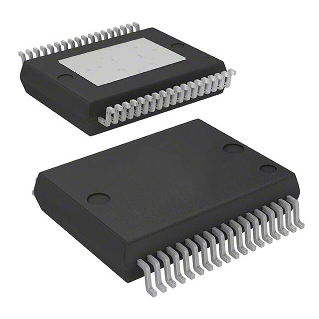
PowerSSO-36
GAPGCFT00004
Features
MultiSense diagnostic functions
– Output short to ground detection
– Thermal shutdown indication
– OFF-state open-load detection
– Output short to VCC detection
Standby mode
Half bridge operation
Type
RDS(on)
Iout
VCCmax
VNHD7008AY
8 mtyp
per channel)
51 A
38 V
Output current: 51 A
Dual fully protected HSD with MultiSense
feedback
Two integrated drivers for the external LSDs
3 V CMOS compatible inputs
Protections:
– Undervoltage shutdown
– Overvoltage clamp
– Thermal shutdown
– Load current limitation
– Self-limiting of fast thermal transients
(Power Limitation)
– Cross current protection
– Shoot through protection
– Loss of ground and loss of VCC
– Electrostatic discharge protection
– Drain and source voltage monitoring of the
external power MOSFETs, configurable via
an external resistance (short-to-battery
protection)
PWM operation up to 20 kHz for external LSDs
April 2020
This is information on a product in full production.
Package: ECOPACK
Description
AEC-Q100 qualified
MultiSense monitoring functions
– Analog motor current feedback
– Chip temperature monitoring
– Battery voltage monitoring
Charge pump output for reverse battery
protection
The device is a DC motor driver for automotive
applications. It integrates a full protected dual
high-side driver and the drivers and protections
for the two external power MOSFETs in low-side
configuration.
The device is designed using STMicroelectronics
well known and proven proprietary VIPower® M0
technology that allows to efficiently integrate on
the same die a true PowerMOSFET with an
intelligent signal/ protection circuitry. The device
is housed in a PowerSSO-36 exposed pad
package to optimize the dissipation
performances.
The input signals INA and INB can directly
interface the microcontroller to select the motor
direction and the brake conditions. Two selection
pins (SEL0 and SEL1) are available to address to
the microcontroller the information available on
the MultiSense. The MultiSense pin allows to
monitor the motor current, provides a voltage
proportional to the battery value and the
information on the temperature of the chip. The
integrated protections are: load current limitation,
overload active power limitation (with latch-off),
overtemperature shutdown (with latch-off) and
cross current protection.
DS11459 Rev 6
1/44
www.st.com
�Contents
VNHD7008AY
Contents
1
Block diagram and pin description . . . . . . . . . . . . . . . . . . . . . . . . . . . . . 6
2
Electrical specifications . . . . . . . . . . . . . . . . . . . . . . . . . . . . . . . . . . . . . . 9
3
2.1
Absolute maximum ratings . . . . . . . . . . . . . . . . . . . . . . . . . . . . . . . . . . . . . 9
2.2
Thermal data . . . . . . . . . . . . . . . . . . . . . . . . . . . . . . . . . . . . . . . . . . . . . . 10
2.3
Electrical characteristics . . . . . . . . . . . . . . . . . . . . . . . . . . . . . . . . . . . . . . .11
2.4
Waveforms . . . . . . . . . . . . . . . . . . . . . . . . . . . . . . . . . . . . . . . . . . . . . . . . 24
Protections . . . . . . . . . . . . . . . . . . . . . . . . . . . . . . . . . . . . . . . . . . . . . . . . 27
3.1
Power limitation (high-side driver) . . . . . . . . . . . . . . . . . . . . . . . . . . . . . . 27
3.2
Thermal shutdown . . . . . . . . . . . . . . . . . . . . . . . . . . . . . . . . . . . . . . . . . . 27
3.3
High-side current limitation . . . . . . . . . . . . . . . . . . . . . . . . . . . . . . . . . . . . 27
3.4
External PowerMOS low side VDS monitoring . . . . . . . . . . . . . . . . . . . . . 27
4
Typical application schematic . . . . . . . . . . . . . . . . . . . . . . . . . . . . . . . . 28
5
MultiSense operation . . . . . . . . . . . . . . . . . . . . . . . . . . . . . . . . . . . . . . . 29
5.1
MultiSense analog monitoring . . . . . . . . . . . . . . . . . . . . . . . . . . . . . . . . . 29
5.2
Multisense diagnostics flag in fault conditions . . . . . . . . . . . . . . . . . . . . . 29
6
VREG and Driver_LS Block . . . . . . . . . . . . . . . . . . . . . . . . . . . . . . . . . . 30
7
Reverse battery protection . . . . . . . . . . . . . . . . . . . . . . . . . . . . . . . . . . . 30
8
Open-load detection in off-state . . . . . . . . . . . . . . . . . . . . . . . . . . . . . . 30
9
Immunity against transient electrical disturbances . . . . . . . . . . . . . . . 31
10
Package and PCB thermal data . . . . . . . . . . . . . . . . . . . . . . . . . . . . . . . 32
10.1
11
2/44
PowerSSO-36 thermal data . . . . . . . . . . . . . . . . . . . . . . . . . . . . . . . . . . . 32
Package and packing information . . . . . . . . . . . . . . . . . . . . . . . . . . . . . 36
11.1
PowerSSO-36 package information . . . . . . . . . . . . . . . . . . . . . . . . . . . . . 36
11.2
PowerSSO-36 packing information . . . . . . . . . . . . . . . . . . . . . . . . . . . . . 38
DS11459 Rev 6
�VNHD7008AY
11.3
Contents
PowerSSO-36 marking information . . . . . . . . . . . . . . . . . . . . . . . . . . . . . 40
12
Order codes . . . . . . . . . . . . . . . . . . . . . . . . . . . . . . . . . . . . . . . . . . . . . . . 41
13
Revision history . . . . . . . . . . . . . . . . . . . . . . . . . . . . . . . . . . . . . . . . . . . 42
DS11459 Rev 6
3/44
3
�List of tables
VNHD7008AY
List of tables
Table 1.
Table 2.
Table 3.
Table 4.
Table 5.
Table 6.
Table 7.
Table 8.
Table 9.
Table 10.
Table 11.
Table 12.
Table 13.
Table 14.
Table 15.
Table 16.
Table 17.
Table 18.
Table 19.
Table 20.
4/44
Block description. . . . . . . . . . . . . . . . . . . . . . . . . . . . . . . . . . . . . . . . . . . . . . . . . . . . . . . . . . 6
Pin definitions and functions . . . . . . . . . . . . . . . . . . . . . . . . . . . . . . . . . . . . . . . . . . . . . . . . . 8
Suggested connection for unused and not connected pins . . . . . . . . . . . . . . . . . . . . . . . . . 8
Absolute maximum ratings . . . . . . . . . . . . . . . . . . . . . . . . . . . . . . . . . . . . . . . . . . . . . . . . . . 9
Thermal data. . . . . . . . . . . . . . . . . . . . . . . . . . . . . . . . . . . . . . . . . . . . . . . . . . . . . . . . . . . . 10
Power section . . . . . . . . . . . . . . . . . . . . . . . . . . . . . . . . . . . . . . . . . . . . . . . . . . . . . . . . . . . 11
Logic inputs (INA, INB) (Vcc = 7 V up to 28 V; -40 °C < Tj < 150 °C) . . . . . . . . . . . . . . . . . 12
HSD switching (VCC = 13 V; RLOAD = 1.1 ) . . . . . . . . . . . . . . . . . . . . . . . . . . . . . . . . . . 13
Gate driver for external MOS parameters (VCC = 13 V) . . . . . . . . . . . . . . . . . . . . . . . . . . . 13
Protections and diagnostics (7 V < VCC < 18 V; -40 °C < Tj < 150 °C). . . . . . . . . . . . . . . . 13
MultiSense (7 V < VCC < 18 V; -40 °C < Tj < 150 °C) . . . . . . . . . . . . . . . . . . . . . . . . . . . . . 15
Operative condition - truth table . . . . . . . . . . . . . . . . . . . . . . . . . . . . . . . . . . . . . . . . . . . . . 22
On-state fault conditions- truth table . . . . . . . . . . . . . . . . . . . . . . . . . . . . . . . . . . . . . . . . . . 22
Off-state — truth table . . . . . . . . . . . . . . . . . . . . . . . . . . . . . . . . . . . . . . . . . . . . . . . . . . . . 23
IISO 7637-2 - electrical transient conduction along supply line . . . . . . . . . . . . . . . . . . . . . 31
PCB properties . . . . . . . . . . . . . . . . . . . . . . . . . . . . . . . . . . . . . . . . . . . . . . . . . . . . . . . . . . 33
Thermal parameters . . . . . . . . . . . . . . . . . . . . . . . . . . . . . . . . . . . . . . . . . . . . . . . . . . . . . . 34
PowerSSO-36 (exposed pad) package mechanical data . . . . . . . . . . . . . . . . . . . . . . . . . . 36
Device summary . . . . . . . . . . . . . . . . . . . . . . . . . . . . . . . . . . . . . . . . . . . . . . . . . . . . . . . . . 41
Document revision history . . . . . . . . . . . . . . . . . . . . . . . . . . . . . . . . . . . . . . . . . . . . . . . . . 42
DS11459 Rev 6
�VNHD7008AY
List of figures
List of figures
Figure 1.
Figure 2.
Figure 3.
Figure 4.
Figure 5.
Figure 6.
Figure 7.
Figure 8.
Figure 9.
Figure 10.
Figure 11.
Figure 12.
Figure 13.
Figure 14.
Figure 15.
Figure 16.
Figure 17.
Figure 18.
Figure 19.
Figure 20.
Figure 21.
Figure 22.
Figure 23.
Figure 24.
Figure 25.
Block diagram . . . . . . . . . . . . . . . . . . . . . . . . . . . . . . . . . . . . . . . . . . . . . . . . . . . . . . . . . . . . 6
Configuration diagram (top view) . . . . . . . . . . . . . . . . . . . . . . . . . . . . . . . . . . . . . . . . . . . . . 7
Current and voltage conventions . . . . . . . . . . . . . . . . . . . . . . . . . . . . . . . . . . . . . . . . . . . . . 9
TDSTKON . . . . . . . . . . . . . . . . . . . . . . . . . . . . . . . . . . . . . . . . . . . . . . . . . . . . . . . . . . . . . . . . . . . . . . . . . . . . . . . . 18
Definition of the low-side switching times . . . . . . . . . . . . . . . . . . . . . . . . . . . . . . . . . . . . . . 19
Definition of the high-side switching times . . . . . . . . . . . . . . . . . . . . . . . . . . . . . . . . . . . . . 19
Low-side turn-on delay time . . . . . . . . . . . . . . . . . . . . . . . . . . . . . . . . . . . . . . . . . . . . . . . . 20
Input reset time for HSD-fault unlatch. . . . . . . . . . . . . . . . . . . . . . . . . . . . . . . . . . . . . . . . . 20
Input reset time for LSD-fault unlatch . . . . . . . . . . . . . . . . . . . . . . . . . . . . . . . . . . . . . . . . . 21
OFF-state diagnostic delay time from rising edge of VOUT (tD_VOL) . . . . . . . . . . . . . . . . 21
Normal operative conditions (resistive load) . . . . . . . . . . . . . . . . . . . . . . . . . . . . . . . . . . . . 24
Out shorted to ground and short clearing . . . . . . . . . . . . . . . . . . . . . . . . . . . . . . . . . . . . . . 25
OUT shorted to Vcc and short clearing. . . . . . . . . . . . . . . . . . . . . . . . . . . . . . . . . . . . . . . . 26
Gate driver low side rise time normalized vs Cg = 4.7nF . . . . . . . . . . . . . . . . . . . . . . . . . . 26
Gate driver low side fall time normalized vs Cg = 4.7nF . . . . . . . . . . . . . . . . . . . . . . . . . . . 26
Typical application schematic . . . . . . . . . . . . . . . . . . . . . . . . . . . . . . . . . . . . . . . . . . . . . . . 28
MultiSense block diagram. . . . . . . . . . . . . . . . . . . . . . . . . . . . . . . . . . . . . . . . . . . . . . . . . . 29
PowerSSO-36 PCB board . . . . . . . . . . . . . . . . . . . . . . . . . . . . . . . . . . . . . . . . . . . . . . . . . 32
Rthj-amb vs PCB copper area in open box free air condition . . . . . . . . . . . . . . . . . . . . . . . 33
Thermal fitting model of a double-channel HSD in PowerSSO-36 . . . . . . . . . . . . . . . . . . . 34
Thermal impedance junction ambient single pulse . . . . . . . . . . . . . . . . . . . . . . . . . . . . . . . 34
PowerSSO-36 package dimensions . . . . . . . . . . . . . . . . . . . . . . . . . . . . . . . . . . . . . . . . . . 36
PowerSSO-36 tube shipment (no suffix) . . . . . . . . . . . . . . . . . . . . . . . . . . . . . . . . . . . . . . 38
PowerSSO-36 tape and reel shipment (suffix “TR”) . . . . . . . . . . . . . . . . . . . . . . . . . . . . . . 39
PowerSSO-36 marking information . . . . . . . . . . . . . . . . . . . . . . . . . . . . . . . . . . . . . . . . . . 40
DS11459 Rev 6
5/44
5
�Block diagram and pin description
1
VNHD7008AY
Block diagram and pin description
Figure 1. Block diagram
VREG
VCC
CP
VBATT
VREG
Reverse
Driver
LSA_OVERTEMPERATURE
HSA_OVERTEMPERATURE
CLAMP HS
OUT A
DRIVER
LS A
B
CURRENT
LIMITATION B
OUT B
1/K
FAULT
DETECTION
CLAMP LS
A
GATE_LSA
HS
Open-load
OFF-state B
1/K
B
DRIVER
HS B
LOGIC
Open-load
OFF-state A
CURRENT
LIMITATION A
CLAMP HS
CP
DRIVER
HS A
HS A
CLAMP LS
HSB_OVERTEMPERATURE
CP
A
Power
Limitation
LSB_OVERTEMPERATURE
UV
B
DRIVER
LS B
MUX
GATE_LSB
VREF_OVL_LSB
VREF_OVL_LSB
VDS_MONITORING
SEL0
IN A
MultiSense_EN
MultiSense
KSOURCE_LSA
SEL1
VDS_MONITORING
KSOURCE_LSB
IN B PWM
GAPG2808151154_2CFT
Table 1. Block description
Name
Description
Logic control
Allows the turn-on and the turn-off of the high-side and the
low-side switches according to the truth table.
Undervoltage (US)
Shuts down the device for battery voltage below (4 V).
High-side and low-side clamp voltage
Protect the high-side and the low-side switches from the high
voltage on the battery line.
High-side and low-side driver
Drive the gate of the concerned switch to allow a proper Ron
for the leg of the bridge.
Current limitation
Limits the motor current in case of short circuit.
In case of short-circuit with the increase of the junction
High-side overtemperature protection temperature, it shuts down the concerned driver to prevent
degradation and to protect the die.
6/44
VDS_MONITORING
Protection of LSD powers against short to battery failure
VREG
Internal voltage regulator that provides the supply for the
gates of the external low-side switches
Fault detection
Signalizes an abnormal condition of the power stage (output
shorted to ground or output shorted to battery) by a feedback
on the MultiSense
DS11459 Rev 6
�VNHD7008AY
Block diagram and pin description
Table 1. Block description (continued)
Name
Description
Power limitation
Limits the power dissipation of the high-side driver inside
safe range in case of short to ground condition.
Open-load in OFF-state
Signalize, in combination with an external resistor, an openload when the switches are off by a feedback on the
MultiSense
Tchip monitoring
Provides a signal linked to the Chip temperature by a
feedback on the MultiSense
VCC monitoring
Provides a signal linked to the Chip temperature by a
feedback on the MultiSense
Reverse driver
Drives an external PowerMOSFET to provide the reverse
battery protection
CP
Charge pump to drive the external N-MOSFET used on the
battery track for the reverse battery protection.
The N-MOSFET source must be connected to the Vbatt pin.
Figure 2. Configuration diagram (top view)
OUTA
OUTA
OUTA
OUTA
OUTA
OUTA
OUTA
OUTA
OUTA
OUTA
SEL0
MultiSense_EN
GATE_LSA
KSOURCE_LSA
VREF_OVL_LSA
INA
CP
Vbatt
1
36
TAB = V CC
18
19
OUTB
OUTB
OUTB
OUTB
OUTB
OUTB
OUTB
OUTB
OUTB
OUTB
SEL1
VREG
GATE_LSB
KSOURCE_LSB
VREF_OVL_LSB
IN B
PWM
MultiSense
GAPG2808151437CFT
DS11459 Rev 6
7/44
43
�Block diagram and pin description
VNHD7008AY
Table 2. Pin definitions and functions
Pin N°
Symbol
Function
20
PWM
PWM input.
25
VREG
Internal supply output
16
INA
Clockwise input.
18
Vbatt
Battery supply, connection to the source of the external
PowerMOS used for the reverse battery protection
19
MultiSense
12
MultiSense_EN
11
SEL0
Address the MultiSense multiplexer (refer to Table 12)
26
SEL1
Address the MultiSense multiplexer (refer to Table 12)
21
INB
1, 2, 3, 4, 5, 6, 7,
8, 9, 10
OUTA
Source of high-side switch A
27, 28, 29, 30, 31,
32, 33, 34, 35, 36
OUTB
Source of high-side switch B
17
CP
15
VREF_OVL_LSA
Sets the threshold for VDS_MONITORING feature for LSA
22
VREF_OVL_LSB
Sets the threshold for VDS_MONITORING feature for LSB
13
GATE_LSA
Gate driver of the external PowerMOS LSA
24
GATE_LSB
Gate driver of the external PowerMOS LSB
14
KSOURCE_LSA
Source of external LSA. Ground connection
23
KSOURCE_LSB
Source of external LSB. Ground connection
TAB
VCC
Output of current sense and diagnostic feedback
Enables the MultiSense diagnostic pin
Counter clockwise input.
Drives the gate of external P-MOSFET for the reverse
battery protection
Supply voltage. Drain of the high-side switches and
connection to the drain of the external PowerMOS used for
the reverse battery protection
Table 3. Suggested connection for unused and not connected pins
Connection / pin
OUTA, OUTB
Inx, PWM, SELx,
Multisense_EN
Multisense
GATE_LSA,
GATE_LSB, CP,
VREG
VREF_OVL_LSA,
VREF_OVL_LSB
Floating
X
X
X
X
X
To ground
Not allowed
Not allowed
X
8/44
Through 10 kΩ resistor
DS11459 Rev 6
�VNHD7008AY
2
Electrical specifications
Electrical specifications
Figure 3. Current and voltage conventions
IS
IB
IDS_LSA
V REF_OVL_LSA
IDS_LSB
Vbatt
CP
OUTA
V REF_OVL_LSB
IINA
ICP
TAB = V CC
OUTB
INA
IINB
MultiSense
INB
GATE_LSA
SEL1
IREG
VREG
PWM
VREG
VSEL1
VSEL0
VINB
VINA
VDS_LSB
VDS_LSA
IPWM
IGLSB
VPWM
VGLSB
GATE_LSB
ISEL1
KSOURCE_LSB
SEL0
KSOURCE_LSA
MultiSense_EN
ISEL0
IGLSA
VGLSA
IOUTA
IOUTB
ISENSE
ISEN
VSEN V
SENSE
VOUTB
VOUTA
VCP
VCC
IGND
GAPG3109150935CFT
2.1
Absolute maximum ratings
Stressing the device above the rating listed in Table 4 may cause permanent damage to the
device. These are stress ratings only and operation of the device at these or any other
conditions above those indicated in the Operating sections of this specification is not
implied. Exposure to Absolute Maximum Rating conditions for extended periods may affect
device reliability.
Table 4. Absolute maximum ratings
Symbol
VCC
Parameter
H-Bridge supply voltage
VBAT
Maximum battery
Imax
DC output current
voltage(1)
Value
Unit
38
V
-16 to 38
V
Internally
limited
A
30
A
IR
Reverse output current (continuous)(2)
IIN
Input current (INA and INB pins)
-1 to 10
mA
ISEL
SEL0,1 DC input current
-1 to 10
mA
IPWM
PWM Input current
-1 to 10
mA
SenseEnable DC input current
-1 to 1.5
mA
MultiSense pin DC output current (VGND = VCC and VSENSE < 0 V)
10
mA
MultiSense pin DC output current in reverse (VCC < 0 V)
-20
mA
VREG DC voltage
12
V
IMultiSense_EN
IMultiSense
VREG
DS11459 Rev 6
9/44
43
�Electrical specifications
VNHD7008AY
Table 4. Absolute maximum ratings (continued)
Symbol
Parameter
VCP
Value
Unit
VBATT -6 to
VBATT +14
V
12
V
-1 to 10
V
2
4
4
kV
Junction operating temperature
-40 to 150
°C
Storage temperature
-55 to 150
°C
100
mA
VCP DC voltage
VGATE_LSx
VREF_OVL_LSx
GATE_LAS, GATE_LSB DC voltage
VREF_OVL_LSA, VREF_OVL_LSB input current
Electrostatic discharge (Human body model: R = 1.5 kΩ; C = 100 pF)
– MultiSenseVREG, VREF_OVL_LSx
– INA, INB, OUTA, OUTB, PWM, SEL0, SEL1, SENSE_EN
– GATE_LSx
VESD
Tc
TSTG
IK_SOURCE_LSx
DC reverse ground pin current (per leg)
1. This applies with the n-channel MOSFET used for the reverse battery protection. Otherwise VBAT has to be shorted to VCC.
2. Based on the internal wires capability.
All logic pins cannot be left floating but they must be connected to GND if unused.
2.2
Thermal data
Table 5. Thermal data
Symbol
Parameter
Unit
Rthj-case
Thermal resistance junction-case (per leg channel)
(JEDEC JESD 51-8)
2.4
°C/W
Rthj-amb
Thermal resistance junction-ambient (JEDEC JESD 51-5)(1)
50.6
°C/W
Rthj-amb
Thermal resistance junction-ambient (JEDEC JESD 51-7)
16.6
°C/W
1. Device mounted on two-layers 2s0p PCB with 2 cm2.heatsink copper trace.
10/44
Max. value
DS11459 Rev 6
�VNHD7008AY
2.3
Electrical specifications
Electrical characteristics
VCC = 7 V up to 28 V; -40 °C < Tj < 150 °C, unless otherwise specified.
Table 6. Power section
Symbol
VCC
IS
tD_STBY
RONHS
Parameter
Test conditions
Operating supply
voltage
Supply current
Standby mode
blanking time
Static high-side
resistance
Min.
4
IL(off)
V
Off-state standby
INA = INB = PWM = Multisense_EN= 0;
SEL0,1 = 0; Tj = 25 °C; VCC = 13 V
1
µA
Off-state standby;
INA = INB = PWM = Multisense_EN= 0;
SEL0,1 = 0; VCC = 13 V; Tj = 85 °C
1
µA
Off-state standby;
INA = INB = PWM = Multisense_EN= 0;
SEL0,1 = 0; VCC = 13 V; Tj = 125 °C
10
µA
Off-state (no standby)
INA = INB = PWM = Multisense_EN= 0;
SEL0,1 = 5 V
4
8
mA
On-state: INA or INB = 5V;
PWM = 0 V or PWM = 5 V;
SEL0 = 0 or SEL0 = 5 V;
SEL1 = 0 or SEL1 = 5 V
6
12
mA
On-state: INA = INB = 5V;
PWM = 0 V or PWM = 5 V;
SEL0 = 0 or SEL0 = 5 V;
SEL1 = 0 or SEL1 = 5 V
9
18
mA
300
550
µs
VCC = 13 V; INA = INB = SEL1 =
MultiSense_EN = PWM = 0 V;
VSEL0 from 5 V to 0 V.
60
IOUT = 12 A; Tj = 25 °C,
VCC = 13 V
8
IOUT = 12 A;
Tj = - 40 °C to 150 °C
IL(off_h)
mΩ
16
mΩ
0.7
V
8
High-side freewheeling diode forward IOUT = -12 A; Tj = 150 °C
voltage
Off-State Output
current of one output
Unit
28
VCC = 4 V, IOUT = 12 A, Tj=25 °C
Vf
Typ. Max.
0.6
INA = INB = PWM = 0; VOUT = 0 V;
VCC = 13 V; Tj = 25 °C
0
0.5
µA
INA = INB = PWM = 0; VOUT = 0 V;
VCC = 13 V; Tj = 125°C
0
5
µA
20
60
µA
Off-state output current
of one output with
INA = PWM = 0; INB = 5 V; VCC = 13 V
other HSD on
DS11459 Rev 6
11/44
43
�Electrical specifications
VNHD7008AY
Table 7. Logic inputs (INA, INB) (Vcc = 7 V up to 28 V; -40 °C < Tj < 150 °C)
Symbol
Parameter
Test conditions
Min.
Typ.
Max.
Unit
0.9
V
VIL
Input low level voltage
VIH
Input high level voltage
2.1
V
VIHYST
Input hysteresis voltage
0.2
V
IIN = 1 mA
VICL
Input clamp voltage
IINL
Input current
VIN = 0.9 V
IINH
Input current
VIN = 2.1 V
5.3
IIN = -1 mA
7.2
-0.7
V
V
1
µA
10
µA
0.9
V
SEL0, SEL1 (VCC = 7 V up to 18 V; -40 °C < Tj < 150 °C)
VSELL
Input low level voltage
ISELL
Low level input current
VSELH
Input high level voltage
ISELH
High level input current
VSEL(hyst)
Input hysteresis voltage
VSELCL
VSEL = 0.9 V
µA
2.1
V
VSEL = 2.1 V
10
0.2
ISEL = 1 mA
Input clamp voltage
1
V
5.3
ISEL = -1 mA
µA
7.2
-0.7
V
V
PWM (VCC = 7 V up to 28 V; -40 °C < Tj < 150 °C)
VPWM
Input low level voltage
IPWM
Low level input current
VPWM
Input high level voltage
IPWMH
High level input current
0.9
VPWM = 0.9 V
VPMWCL
µA
2.1
V
10
0.2
IPWM = 1 mA
Input clamp voltage
1
VPWM = 2.1 V
VPWM(hyst) Input hysteresis voltage
V
V
5.3
IPWM = -1 mA
µA
7.2
-0.7
V
V
MultiSense_EN (VCC = 7 V up to 18 V; -40 °C < Tj < 150 °C)
VSEnL
Input low level voltage
ISEnL
Low level input current
VSEnH
Input high level voltage
ISEnH
High level input current
VSEn(hyst)
Input hysteresis voltage
VSEnCL
12/44
Input clump voltage
0.9
VSEn = 0.9 V
1
µA
2.1
V
VSEn = 2.1 V
10
0.2
ISEn = 1 mA
ISEn = -1 mA
DS11459 Rev 6
V
µA
V
5.3
7.5
-0.7
V
V
�VNHD7008AY
Electrical specifications
Table 8. HSD switching (VCC = 13 V; RLOAD = 1.1 )
Symbol
td(on)
td(off)
Parameter
Test conditions
Min.
Typ.
Max.
Unit
Turn-on delay time
Input rise time < 1 µs;
MultiSense_EN = 5 V (no
standby); SEL0,1 = 0; PWM = 0
(see Figure 6)
53
µs
Turn-off delay time
Input rise time < 1 µs;
MultiSense_EN = 5 V (no
standby); SEL0,1 = 0; PWM = 0
(see Figure 6)
20
µs
Table 9. Gate driver for external MOS parameters (VCC = 13 V)
Symbol
f(1)
Parameter
Test conditions
Min.
PWM frequency
Typ.
Max.
Unit
20
kHz
10
V
0
PWM = 5 V; INx = 0 V
Vgs_lsd
Gate_LSD voltage
VCC = 4 V, PWM = 5 V,
INx = 0 V, Tj=25 °C
tcross
Low-side turn-on delay time
Input rise time < 1 µs
(see Figure 7)
tgr_ls
Rise time
tgf_ls
Fall time
4
40
V
160
300
µs
VCC = 13.5 V; Rg = 0 Ω;
Cg = 4.7 nF
(see Figure 5)
0.25
0.5
µs
VCC = 13.5 V; Rg = 0 Ω;
Cg = 4.7 nF
(see Figure 5)
0.35
0.5
µs
1. Parameter guaranteed by design.
Table 10. Protections and diagnostics (7 V < VCC < 18 V; -40 °C < Tj < 150 °C)
Symbol
Max.
Unit
VCC falling
4
V
VUSDreset
Undervoltage shutdown reset VCC rising
5
V
VUSDhyst
Undervoltage shutdown
hysteresis
ILIM_HSD
High-side current limitation
VCL_HSD
High-side driver clamp
voltage (VCC to OUTA = 0 or
OUTB = 0)
VUSD
VCL_LSD(1)
tDEL_OVL_LSD
Parameter
Test conditions
Undervoltage shutdown
Min.
Typ.
0.3
51
VCC = 4 V, Tj=25 °C
(1)
77
110
A
66
A
V
IOUT = 100 mA;
tclamp = 1 ms;
Iclamp = 100 mA
38
46
IOUT = 100 mA;
Low-side clamp voltage
(OUTA = VCC or OUTB = VCC tclamp = 1 ms;
to GND)
Iclamp = 100 mA
38
46
Low-side drain-current
overload blanking time
1
DS11459 Rev 6
V
52
V
5
µs
13/44
43
�Electrical specifications
VNHD7008AY
Table 10. Protections and diagnostics (7 V < VCC < 18 V; -40 °C < Tj < 150 °C) (continued)
Symbol
Min.
Typ.
Max.
Unit
40
50
60
µA
Low-side drain-current
VREF_OVL_LSD_MIN overload threshold voltage
minimum
0.32
0.4
0.8
V
Low-side drain-current
VREF_OVL_LSD_MAX overload threshold voltage
maximum
1.6
2
2.4
V
150
175
200
°C
IREF_OVL_LSD
High-side thermal shutdown
temperature
TTR_HSD
High-side thermal reset
temperature
ΔTj_SD(1)
IL(off3)
Test conditions
Low-side drain-current
overload reference current
TTSD_HSD
THYST_HSD
INx = 2.1 V
135
°C
High-side thermal hysteresis
(TSD_HSD - TR_HSD)
7
°C
Dynamic temperature
60
°C
OFF-state output sink current INA = INB = 0; PWM = 0;
with VOUT = VCC
VOUT = VCC
0
1.1
2.5
mA
VCL
Clamp signal
(VCC to GND)
IOUT = 100 mA;
tclamp = 1 ms;
Iclamp = 100 mA
38
46
52
V
VOL
OFF-state open-load voltage
detection threshold
INA = INB = 0; PWM = 0;
VSEL0 = 5 V for CHA;
VSEL0 = 0 V and within
tD_STBY for CHB
2
3
4
V
-5
µA
IL(off2)
tDSTKON
INA = INB = 0; VOUT = 2 V;
PWM = 2 V;
OFF-state output sink current VSEL0 = 5 V for CHA;
VSEL0 = 0 V and within
tD_STBY for CHB
OFF-state diagnostic delay
time from falling edge of
INPUT (see Figure 4)
-150
INA = 5 V to 0 V; INB = 0;
PWM = 0; VSEL0 = 5 V;
IOUT = 0 A; VOUTA = 4 V
40
160
300
µs
VCP - VBAT = VGS_CP
8
12
15
V
VGS_CP
CP output voltage
tD_VOL
INA = INB = 0 V; PWM = 0;
OFF-state diagnostic delay
VOUTx = 0 V to 4 V;
time from rising edge of VOUT VSEL1 = 0 V for CHA;
(see Figure 10)
VSEL0,1 = 0 V;
SENSE_EN = 5 V for CHB
tLATCH_RST_HS
14/44
Parameter
VBAT = -16 V;
VCP - VBAT = VGS_CP
Input reset time for high-side
fault unlatch
VINx = 5 V to 0 V; HSDx
faulting (see Figure 8)
DS11459 Rev 6
0.6
3
V
5
30
µs
10
20
µs
�VNHD7008AY
Electrical specifications
Table 10. Protections and diagnostics (7 V < VCC < 18 V; -40 °C < Tj < 150 °C) (continued)
Symbol
tLATCH_RST_LS
tstby_ovl_lsd
Parameter
Input reset time for low-side
fault unlatch
Test conditions
Min.
Typ.
Max.
Unit
3
10
20
µs
VINx = 0 V to 5 V; LSDx
faulting (see Figure 9)
Low-side drain current
overload delay time form stby 50% of VSENSEH
exit
20
µs
1. Parameter guaranteed by design and characterization; not subject to production test.
Table 11. MultiSense (7 V < VCC < 18 V; -40 °C < Tj < 150 °C)
Symbol
VSENSE_CL
Parameter
MultiSense clamp
voltage
Test conditions
Min.
VSEn = 0 V; ISENSE = -1 mA
VSEn = 0 V; ISENSE = 1 mA
Typ.
Max.
7
-17
Unit
V
-12
V
KOL
IOUT/ISENSE
IOUT = 0.25 A; VSENSE = 0.5 V
Tj = -40 °C to 150 °C
6300
10500
14700
K0
IOUT/ISENSE
IOUT = 2 A; VSENSE = 0.5 V;
Tj = -40 °C to 150 °C
8400
10900
13400
K1
IOUT/ISENSE
IOUT = 6 A; VSENSE = 0.5
Tj = -40 °C to 150 °C
8700
11000
13200
K2
IOUT/ISENSE
IOUT = 12 A; VSENSE = 4 V;
Tj = -40 °C to 150 °C
9000
11000
13000
K3
IOUT/ISENSE
IOUT = 24 A; VSENSE = 4 V
Tj = -40 °C to 150 °C
9200
11000
12200
dKOL/KOL(1)
Analog sense
current drift
IOUT = 0.25 A; VSENSE = 0.5 V;
Tj = -40 °C to 150 °C
-25
25
%
dK0/K0(1)
Analog sense
current drift
IOUT = 2 A; VSENSE = 0.5 V;
VSENSE_EN = 0 V;
Tj = -40 °C to 150 °C
-5
5
%
dK1/K1(1)
Analog sense
current drift
IOUT = 6 A; VSENSE = 0.5 V;
VSENSE_EN = 0 V;
Tj = -40 °C to 150 °C
-5
5
%
dK2/K2(1)
Analog sense
current drift
IOUT = 12 A; VSENSE = 4 V;
Tj = -40 °C to 150°C
-5
5
%
dK3/K3(1)
Analog sense
current drift
IOUT = 24 A; VSENSE = 4 V;
Tj = -40 °C to 150°C
-5
5
%
VSENSE_SAT
Max analog sense
output voltage
VCC = 7 V; RSENSE = 10 kΩ;
IOUT = 24 A; VSEL0 = 5 V;
Tj = 150 °C
5
V
ISENSE_SAT(2)
MultiSense
saturation current
VCC = 7 V; VINA = 5 V; VINB = 0 V;
VSEL0 = 5 V; Tj = 150°C
4
mA
IOUT_SAT(2)
Output saturation
current
VCC = 7 V; VSENSE = 4 V;
VINA = 5 V; VINB = 0 V; VSEL0 = 5 V;
Tj = 150°C
48
A
DS11459 Rev 6
15/44
43
�Electrical specifications
VNHD7008AY
Table 11. MultiSense (7 V < VCC < 18 V; -40 °C < Tj < 150 °C) (continued)
Symbol
VOUT_MSD(2)
ISENSE0
Parameter
Output Voltage for
MultiSense
shutdown
MultiSense leakage
current
Test conditions
Min.
VINA = 5 V; VINB = 0 V; VSEL0 = 5 V;
VSEL1 = 0 V; RSENSE = 2.7 kΩ
IOUT = 24 A
Typ.
Max.
5
Unit
V
VMultiSense = VSENSE_EN = PWM = 0
V; INA = INB =0 V; SEL0 = SEL1 = 0;
Tj = -40 °C to 150°C (standby)
0
0.5
µA
SEn = 5 V; INA = INB = 5 V;
PWM = 0 V; SideX diagnostic
selected; IOUTx = 0 A
E.g.
– SideA: SEL0 = 5 V; SEL1 = 0 V;
IOUTA = 0 A; IOUTB = 12 A
– SideB: SEL0 = 0 V; SEL1 = 0 V;
IOUTA = 12 A; IOUTB = 0 V
0
12
µA
SEn = 5 V; PWM = 0 V; SideX
diagnostic selected; HSx OFF
E.g.
– SideA: SEL0 = 5 V; SEL1 = 0 V;
INA = 0 V; INB = 5 V; IOUTB = 12 A
– SideB: SEL0 = 0 V; SEL1 = 0 V;
INA = 5 V; INB = 0 V; IOUTA = 12 A
0
10
µA
7
V
VSENSEH
MultiSense output
voltage in fault
condition
VCC = 13 V; RSENSE = 1 kΩ;
– E.g: Ch0 in open-load; VIN = 0 V;
IOUT = 0 A; VOUT = 4 V
5
ISENSEH
MultiSense current
in fault condition
9 V < VCC < 18 V;
VSENSE = 5 V; MultiSense in fault
condition
10
20
30
mA
VSENSE_EN = 5 V; VSEL0 = 0 V;
VSEL1 = 5 V; VIN = 0 V;
RSENSE = 1 kΩ; Tj = -40 °C
2.325
2.41
2.495
V
VSENSE_EN = 5 V; VSEL0 = 0 V;
VSEL1 = 5 V; VIN = 0 V;
RSENSE = 1 kΩ; Tj = 25 °C
1.985
2.07
2.155
V
VSENSE_EN = 5 V; VSEL0 = 0 V;
VSEL1 = 5 V; VIN = 5 V;
RSENSE = 1 kΩ; Tj = 125 °C
1.435
1.52
1.605
V
Chip temperature analog feedback
VSENSE_TC
dVSENSE_TC/dT
(2)
MultiSense output
voltage proportional
to chip temperature
Temperature
coefficient
Transfer function
Tj = -40 °C to 150 °C
VSENSE_TC(T) = VSENSE_TC(T0) + dVSENSE_TC/dT * (T - T0)
VCC supply voltage analog feedback
16/44
-5.5
DS11459 Rev 6
mV/K
�VNHD7008AY
Electrical specifications
Table 11. MultiSense (7 V < VCC < 18 V; -40 °C < Tj < 150 °C) (continued)
Symbol
Parameter
Test conditions
Min.
Typ.
Max.
Unit
VSENSE_VCC
MultiSense output
voltage proportional
to VCC supply
voltage
VCC = 13 V; VSENSE_EN = 5 V;
VSEL0 = VSEL1 = 5 V; RSENSE = 1 kΩ
3.16
3.23
3.3
V
tD_CStoTC
VINA = 5 V; VSENSE_EN = 5 V;
MultiSense
VSEL0 = 5 V to 0 V;
transition delay from
VSEL1 = 0 V to 5 V; IOUTA = 2.5 A;
current sense to TC
RSENSE = 1 kΩ; VSENSE_TC = 90% of
sense
VSENSE_TC_FINAL
60
µs
tD_TCtoCS
VINA = 5 V; VSENSE_EN = 5 V;
MultiSense
VSEL0 = 0 V to 5 V;
transition delay from
VSEL1 = 5 V to 0 V; IOUTA = 2.5 A;
TC sense to current
RSENSE = 1 kΩ; ISENSE = 90% of
sense
ISENSE_MAX
20
µs
tD_CStoVCC
VINA = 5 V; VSENSE_EN = 5 V;
MultiSense
VSEL0 = 5 V; VSEL1 = 0 V to 5 V;
transition delay from
I
= 2.5 A; RSENSE = 1 kΩ;
current sense to VCC OUTA
VSENSE_VCC = 90% of
sense
VSENSE_VCC_FINAL
60
µs
tD_VCCtoCS
MultiSense
transition delay from
VCC sense to current
sense
VINA = 5 V; VSENSE_EN = 5 V;
VSEL0 = 5 V; VSEL1 = 5 V to 0 V;
IOUTA = 2.5 A; RSENSE = 1 kΩ;
ISENSE = 90% of ISENSE_MAX
20
µs
tD_TCtoVCC
MultiSense
transition delay from
TC sense to VCC
sense
VCC = 13 V; Tj = 125 °C;
VSENSE_EN = 5 V;
VSEL0 = 0 V to 5 V;
VSEL1 = 5 V; RSENSE = 1 kΩ;
VSENSE_VCC = 90% of
VSENSE_VCC_FINAL
20
µs
tD_VCCtoTC
MultiSense
transition delay from
VCC sense to TC
sense
VCC = 13 V; Tj = 125 °C;
VSENSE_EN = 5 V;
VSEL0 = 5 V to 0 V;
VSEL1 = 5 V; RSENSE = 1 kΩ;
VSENSE_TC = 90% of
VSENSE_TC_FINAL
20
µs
60
µs
VSENSE_VCC = VCC/4
Transfer function
MultiSense timings (Multiplexer transition times)(2)
MultiSense timings (CurrentSense mode)
tDSENSE1H
Current sense
settling time from
rising edge of
VSENSE_EN
VINA = 5 V; VINB = 0 V;
VSENSE_EN = 0 V to 5 V;
RSENSE = 1 k; RL = 2.6 Ω
VPWM = 5 V; VSEL0 = 5 V;
VSEL1 = 0 V
DS11459 Rev 6
17/44
43
�Electrical specifications
VNHD7008AY
Table 11. MultiSense (7 V < VCC < 18 V; -40 °C < Tj < 150 °C) (continued)
Symbol
Parameter
Test conditions
Min.
Typ.
Max.
Unit
tDSENSE1L
Current sense
disable delay time
from falling edge of
VSENSE_EN
VINA = 5 V; VINB = 0 V;
VSENSE_EN = 5 V to 0 V;
RSENSE = 1 k; RL = 2.6 Ω
VPWM = 5 V; VSEL0 = 5 V;
VSEL1 = 0 V
20
µs
tDSENSE2H
VSENSE_TC settling
time from rising
edge of VSENSE_EN
VSENSE_EN = 0 V to 5 V;
VSEL0 = 0 V; VSEL1 = 5 V;
RSENSE = 1 kΩ
60
µs
tDSENSE2L
VSENSE_TC settling
time from rising
edge of VSENSE_EN
VSENSE_EN = 5 V to 0 V;
VSEL0 = 0 V; VSEL1 = 5 V;
RSENSE = 1 kΩ
20
µs
MultiSense timings (VCC voltage sensor mode)
tDSENSE3H
VSENSE_VCC settling VSENSE_EN = 0 V to 5 V;
time from rising
VSEL0 = 5 V; VSEL1 = 5 V;
edge of VSENSE_EN RSENSE = 1 kΩ
60
µs
tDSENSE3L
VSENSE_VCC settling VSENSE_EN = 5 V to 0 V;
time from rising
VSEL0 = 5 V; VSEL1 = 5 V;
edge of VSENSE_EN RSENSE = 1 kΩ
20
µs
1. Analog sense current drift is deviation of factor K for a given device over (-40°C to 150°C and 9 V < VCC < 18 V) with
respect to its value measured at Tj = 25 °C, VCC = 13 V.
2. Parameter guaranteed by design and characterization; not subject to production test.
Figure 4. TDSTKON
VINPUT
VOUT
VOUT > VOL
MultiSense
TDSTKON
18/44
DS11459 Rev 6
GAPGCFT00601
�VNHD7008AY
Electrical specifications
Figure 5. Definition of the low-side switching times
PWM
t
VGATE_LSA,LSB
80%
tgf_Is
80%
20%
20%
tgr_Is
t
Figure 6. Definition of the high-side switching times
VINA
tD(off)
tD(on)
t
VOUTA
90%
10%
t
DS11459 Rev 6
19/44
43
�Electrical specifications
VNHD7008AY
Figure 7. Low-side turn-on delay time
INA
t
INB
t
PWM
t
Gate_LSA
tcross
t
Gate_LSB
t
GAPG3108151219CFT
Figure 8. Input reset time for HSD-fault unlatch
INA
OUTA
Reset Pulse
Fault HSA
Fault removing
Fault cleaning
Multisense
Vmulti_senseH
Tlatch_RST_HSD
Vsense_nom
GAPG2810151219CFT
Note:
20/44
Multisense_EN=1
DS11459 Rev 6
�VNHD7008AY
Electrical specifications
Figure 9. Input reset time for LSD-fault unlatch
INA
OUTA
Reset Pulse
tcross
Fault LSA
OutA Short to VCC
Fault removing
Multisense
Vmulti_senseH
Fault cleaning
T_Lacht_RST_LSD
GAPG2810151222CFT
Note:
Multisense_EN=1
Figure 10. OFF-state diagnostic delay time from rising edge of VOUT (tD_VOL)
INA
Fault : V out> V oL
OUTA
V multi_senseH
Multisense
t D_VOL
GAPG2810151228CFT
Note:
Multisense_EN=1
DS11459 Rev 6
21/44
43
�Electrical specifications
VNHD7008AY
Table 12. Operative condition - truth table
INA INB PWM SEL0 SEL1 MultiSense_EN
MultiSense
HSA
LSA
HSB
LSB
1
0
0
1
High-Z
OFF
ON
OFF
ON
1
1
0
1
High-Z
OFF
ON
OFF
ON
0
0
0
1
Current Monitoring HSB
OFF
OFF
ON
OFF
1
0
0
1
Current Monitoring HSB
OFF
ON
ON
OFF
0
1
0
1
High-Z
OFF
OFF
ON
OFF
1
1
0
1
High-Z
OFF
ON
ON
OFF
0
0
0
1
High-Z
ON
OFF
OFF
OFF
1
0
0
1
High-Z
ON
OFF
OFF
ON
0
1
0
1
Current Monitoring HSA
ON
OFF
OFF
OFF
1
1
0
1
Current Monitoring HSA
ON
OFF
OFF
ON
0
0
1
Current Monitoring HSB
ON
OFF
ON
OFF
1
0
1
Current Monitoring HSA
ON
OFF
ON
OFF
0
1
0
1
Off-state diagnostic OUTA
OFF
OFF
OFF
OFF
0
0
0
0
1
Off-state diagnostic OUTB
OFF
OFF
OFF
OFF
X
X
X
0
1
1
TCHIP Monitoring
—
—
—
—
X
X
X
1
1
1
VCC Monitoring
—
—
—
—
—
—
—
—
0
0
0
1
0
1
1
0
1
0
1
1
X(1)
0
0
0
X
X
X
X
X
0
High-Z
(2)
1. X: the level of the pin can be 0 or 1.
2. When INA = INB = PWM = SEL0 = SEL1 = MultiSense_EN = 0 device enters standby after TDSTBY.
Table 13. On-state fault conditions- truth table
Digital input pins(1)
MultiSense
Comment
0
VSENSE_H
VDS LSB protection triggered; LSB latched off
1
1
VSENSE_H
VDS LSA protection triggered; LSA latched off
1
X
0
VSENSE_H
HSB protection triggered; HSB latched off
0
1
1
1
VSENSE_H
VDS LSA protection triggered; LSA latched off
1
0
1
0
VSENSE_H
VDS LSB protection triggered; LSB latched off
1
0
X
1
VSENSE_H
HSA protection triggered; HSA latched off
1
1
X
0
VSENSE_H
HSB protection triggered; HSB latched off
1
1
X
1
VSENSE_H
HSA protection triggered; HSA latched off
INA
INB
PWM
SEL0
0
0
1
0
0
0
1. MultiSense_EN = 1 and SEL1 = 0 are mandatory for fault detection. Other logic combinations on digital input pins not
reported on the above table do not allow to detect a latched-off channel.
22/44
DS11459 Rev 6
�VNHD7008AY
Electrical specifications
MultiSense
MultiSense_EN
OUTB
OUTA
PWM
SEL1
SEL0
INB
INA
Table 14. Off-state — truth table
Description
VSENSEH
Case 1: OUTA shorted to VCC if no pull-up is applied.
Case 2: NO open-load in full bridge configuration with
an external pull-up on OUTB
Case 3: open-load in half bridge configuration with an
external pull-up on OUTA (motor connected between
Out and Ground)
Hi-Z
Case 1: open-load in full Bridge configuration with an
external pull-up on OUTB
Case 2: NO open-load in half Bridge configuration
with external pull-up on OUTA (motor connected
between Out and Ground)
VSENSEH
Case 1: OUTB shorted to VCC if no pull-up is applied
Case 2: NO open-load in full bridge configuration with
external pull-up on OUTA
Case 3: open-load in half bridge configuration with
external pull-up on OUTB (motor connected between
Out and Ground)
Hi-Z
Case1: open-load in full Bridge configuration with an
external pull-up on OUTA
Case 2. NO open-load in half Bridge configuration
with external pull-up on OUTB (motor connected
between Out and Ground)
VOUTA > VOL
Off-state diagnostic
0
X
0
0
X
Note:
VOUTB > VOL
0
X
VOUTB < VOL
0
1
0
VOUTA < VOL
1
X
1
1
1
To power on the device from standby, it is recommended to: toggle INA or INB or SEL0 or
SEL1 from 0 to 1 first to come out from STBY mode; toggle PWM from 0 to 1 with a delay of
20 microsecond this avoids any overstress on the device in case of existing short-to-battery.
DS11459 Rev 6
23/44
43
�Electrical specifications
2.4
VNHD7008AY
Waveforms
Figure 11. Normal operative conditions (resistive load)
VINA
VINB
VPWM
VSEL0
VOUTA
VOUTB
ILoad
Vsense
GAPG2909150752CFT
Note:
24/44
MultiSense_EN=1
DS11459 Rev 6
�VNHD7008AY
Electrical specifications
Figure 12. Out shorted to ground and short clearing
Outx Shorted To Gnd + Fault Clearing
VINA
Reset Pulse
OutA Shorted to Gnd
Fault Removing
VINB
Reset Pulse
OutB Shorted to Gnd
Fault Removing
VPWM
VSEL0
VOUTA
VOUTB
Vsense_nom
VSenseH
ILoad_nom
VSENSE
ILOAD
GAPG2909150739CFT
Note:
MultiSense_EN=1
DS11459 Rev 6
25/44
43
�Electrical specifications
VNHD7008AY
Figure 13. OUT shorted to Vcc and short clearing
Outx Shorted To Vcc + Fault Clearing
VINA
Reset Pulse
VINB
Fault Removing
OutA Shorted to Vcc
Reset Pulse
Fault Removing
OutB Shorted to Vcc
VPWM
VSEL0
VOUTA
VOUTB
VSENSE
VSenseH
ILOAD
ILoad_nom
GAPG2909150743CFT
Note:
MultiSense_EN=1
Figure 14. Gate driver low side rise time
normalized vs Cg = 4.7nF
tr
GADG271020171146IDL
tf
1
1
0.8
0.8
0.6
0.6
0.4
0.4
0.2
0.2
0
0
26/44
Figure 15. Gate driver low side fall time
normalized vs Cg = 4.7nF
1
2
3
4
Qg(nF)
DS11459 Rev 6
0
0
GADG271020171151LSG
1
2
3
4
Cg (nF)
�VNHD7008AY
Protections
3
Protections
3.1
Power limitation (high-side driver)
The basic working principle of this protection consists of an indirect measurement of the
junction temperature swing Δ Tj through the direct measurement of the spatial temperature
gradient on the device surface in order to automatically shut off the output MOSFET as soon
as Δ Tj exceeds the safety level of Δ Tj_SD. The protection prevents fast thermal transient
effects and, consequently, reduces thermo-mechanical fatigue. When Power Limitation is
reached, The device enters in latch mode and generates the Fault Flag on Multisense =
VsenseH when the faulty leg diagnostic is selected (please refer to Table 13).
3.2
Thermal shutdown
In case the junction temperature of the device exceeds the maximum allowed threshold
(typically 175°C), the device enters in latch mode and generates the Fault Flag on
Multisense = VsenseH (please refer to Table 13). The concerned high side can be switched
ON again as soon as: Tj drops below TTR_HSD, INX is set low for a duration >
TLATCH_RST_HS and set high again.
3.3
High-side current limitation
The device is equipped with an output current limiter in order to protect the silicon as well as
the other components of the system (e.g. bonding wires, wiring harness, connectors, loads,
etc.) from excessive current flow. In case of short circuit, overload or during load power-up,
the output current is clamped to a safety level, ILIMH, by operating the output power
MOSFET in the active region
3.4
External PowerMOS low side VDS monitoring
The VDS_monitoring function has the ability to sense the OUTPUT Mosfet source voltage
and compare it to a predetermined threshold. This threshold is programmable, using an
internal reference current IREF_OVL_LSD = 50 µA (typ.) and an external resistor connected
at VREF_OVL_LS external pin.
This protection will be activated when the low side Power Mos is switched ON and its gate is
fully charged: to guarantee this condition the function will detect a short to battery event only
when PWM = H and after a blanking time tfil_OVL_LS= 2.2 µs (typ.) starting from PWM
rising edge. This feature is present for each LSD leg.
In case of fault conditions caused by Power Limitation or overtemperature or open
load/short to VCC in OFF state, the fault is indicated by the MultiSense pin being internally
switched to a "current limited" voltage source pulled to level VSENSEH.
DS11459 Rev 6
27/44
43
�Typical application schematic
4
VNHD7008AY
Typical application schematic
Figure 16. Typical application schematic
VBAT
4.7K
VBAT
1k
PWM
1k
1k
INB
INA
1k
SEL0
1k
1k
SEL1
MS_EN GATE_LSA
CP
Vcc
100nF
470μF
μC
GATE_LSB
Source_LSB
Vref_OVL_LSB
Vref_OVL_LSA
10K
10K
Note:
1.5K
33nF
VREG
100nF
To protect the device against Battery disconnection with energized inductive load when the
bridge driver goes into 3-state, suggested C(Vcc) is:
Emotor
c V cc = ---------------------------------------20.5DVcc,max
where:
Emotor = 33.5 mJ;
DVcc,max = Vcc_AMR - Vcc_max;
Vcc_AMR = 38 V;
Vcc_max = 26 V (Vcc at jump start);
C(Vcc) = 470 µF
28/44
Open load in off
stete detection
circuity
OUTB
Source_LSA
MS
10k
OUTA
DS11459 Rev 6
�VNHD7008AY
MultiSense operation
5
MultiSense operation
5.1
MultiSense analog monitoring
Diagnostic information on device and load status are provided by an analog output pin
(MultiSense) delivering the following signals:
Current monitor: current mirror of HSDx output current
VCC monitor: voltage propotional to VCC
TCASE: voltage propotional to chip temperature
Those signals are routed through an analog multiplexer which is configured and controlled
by means of SELx and SEn pins, according to the address map in Table 12.
Figure 17. MultiSense block diagram
Vcc
INPUT
Sense MOS
Main MOS
OUT
Current sense
Vbat Monitor
Multisense Switch Block
Temperature monitor
Fault
MULTISENSE
To uC ADC
RPROT
RSENSE
GAPGCFT01040
5.2
Multisense diagnostics flag in fault conditions
Multisense pin delivers fixed voltage (VSENSEH) with a certain current capability in case of:
fault condition on activated high-side triggered by Power Limitation
fault condition on activated high-side triggered by overtemperature protection
fault condition on VDS of Low side exceeded threshold
DS11459 Rev 6
29/44
43
�VREG and Driver_LS Block
6
VNHD7008AY
VREG and Driver_LS Block
VREG pin is the output of an internal low drop voltage regulator. VREG block is designed to
power the driver of external power Mosfet (Driver_LS) and it allows a proper MOS transition.
VREG out voltage will be VREG=10V if Vbattery > 10V, while VREG = Vbattery if
Vbattery < 10V.
An external capacitor CREG = 100 nF connected to the pin VREG is needed to proper
polarize the circuit (see Figure 16).
7
Reverse battery protection
CP pin provides the necessary gate drive for an external n-channel PowerMOS used for
reverse polarity protection. The external N-channel Power MOSFET used for the reverse
battery protection should have the following characteristics:
8
BVdss > 20 V (for a reverse battery of -16 V);
RDS(on) < 1/3 of H-bridge total RDS(on)
Standard Logic Gate Driving
Open-load detection in off-state
The Open Load (OL) detection in off-state operates when output is deactivated (means INA
= INB = PWM=0, or INB together with PWM=0). Open load detection is performed by
reading the MultiSense output. External (switched) pull-up resistor has to be used and
dimensioned to pull output voltage above the maximum open load detection voltage (VOL
MAX) when load is not connected and as well stays below the minimum level (VOL MIN)
when load is connected.
When the open load is detected, VsenseH is indicated on Multisense pin, possible
conditions are specified in Table 14.
If pull up resistor is applied over switched circuitry, it allows to detect short to VCC from
open-load (see Figure 16).
The RPU value has to be:
V BATTmin – V OLmax
R pull_up ----------------------------------------------------------2 I L(off2)min [@VOLmax]
30/44
DS11459 Rev 6
�VNHD7008AY
9
Immunity against transient electrical disturbances
Immunity against transient electrical disturbances
The immunity of the device against transient electrical emissions, conducted along the
supply lines and injected into the VCC pin, is tested in accordance with ISO7637-2:2011 (E)
and ISO 16750-2:2010.
The related function performance status classification is shown in Table 15.
Test pulses are applied directly to DUT (Device Under Test) both in ON and OFF-state and
in accordance to ISO 7637-2:2011(E), chapter 4. The DUT is intended as the present device
only, without components and accessed through VCC and GND terminals.
Status II is defined in ISO 7637-1 Function Performance Status Classification (FPSC) as
follows: "The function does not perform as designed during the test but returns automatically
to normal operation after the test".
Table 15. IISO 7637-2 - electrical transient conduction along supply line
Test pulse
2011(E)
Test pulse severity level
with status II functional
performance status
Minimum
number of
pulses or
test time
Burst cycle/pulse
repetition time
Pulse duration
and pulse
generator
internal
impedance
Level
US(1)
1
III
-112 V
500 pulses
0.5 s
2a
III
+55
500 pulses
0.2 s
5s
50 µs, 2 Ω
3a
IV
-220 V
1h
90 ms
100 ms
0.1 µs, 50 Ω
3b
IV
+150 V
1h
90 ms
100 ms
0.1 µs, 50 Ω
(2)
IV
-7 V
1 pulse
4
min.
max.
2 ms, 10 Ω
100 ms, 0.01 Ω
Load dump according to ISO 16750-2:2010
Test B(3)
40 V
5 pulse
1 min
400 ms, 2 Ω
1. US is the peak amplitude as defined for each test pulse in ISO 7637-2:2011(E)
2. Test pulse from ISO 7637-2:2004(E)
3. With 40 V external suppressor referred to ground (-40 °C < TJ < 150 °C)
DS11459 Rev 6
31/44
43
�Package and PCB thermal data
VNHD7008AY
10
Package and PCB thermal data
10.1
PowerSSO-36 thermal data
Figure 18. PowerSSO-36 PCB board
32/44
DS11459 Rev 6
�VNHD7008AY
Package and PCB thermal data
Table 16. PCB properties
Dimension
Board finish thickness
Value
1.6 mm +/- 10%
Board dimension
129 mm x 86 mm
Board material
FR4
Cu thickness (outer layers)
0.070 mm
Cu thickness (inner layers)
0.035 mm
Thermal via separation
1.2 mm
Thermal via diameter
0.3 mm +/- 0.08 mm
Cu thickness on vias
0.025 mm
Footprint dimension
4.1 mm x 6.5 mm
Figure 19. Rthj-amb vs PCB copper area in open box free air condition
Equation 1: pulse calculation formula
ZTHδ = RTH · δ + ZTHtp (1 - δ)
where δ = tP/T
DS11459 Rev 6
33/44
43
�Package and PCB thermal data
VNHD7008AY
Figure 20. Thermal fitting model of a double-channel HSD in PowerSSO-36
GAPGCFT00325
Note:
The fitting model is a simplified thermal tool and is valid for transient evolutions where the
embedded protections (power limitation or thermal cycling during thermal shutdown) are not
triggered.
Figure 21. Thermal impedance junction ambient single pulse
Table 17. Thermal parameters
Area / island
34/44
FP
2
8
4L
R1 (°C/W)
0.75
R2 (°C/W)
1
R3 (°C/W)
2
2
2
1
R4 (°C/W)
7
6
6
4
R5 (°C/W)
20
14
10
2
DS11459 Rev 6
�VNHD7008AY
Package and PCB thermal data
Table 17. Thermal parameters (continued)
Area / island
FP
2
8
4L
R6 (°C/W)
30
26
15
7
R7 (°C/W)
0.75
R8 (°C/W)
1
C1 (W•s/°C)
0.0027
C2 (W•s/°C)
0.006
C3 (W•s/°C)
0.05
0.05
0.05
0.05
C4 (W•s/°C)
0.15
0.2
0.2
0.2
C5 (W•s/°C)
1
2
3
10
C6 (W•s/°C)
3
5
9
18
C7 (W•s/°C)
0.0027
C8 (W•s/°C)
0.006
DS11459 Rev 6
35/44
43
�Package and packing information
11
VNHD7008AY
Package and packing information
In order to meet environmental requirements, ST offers these devices in different grades of
ECOPACK packages, depending on their level of environmental compliance. ECOPACK
specifications, grade definitions and product status are available at: www.st.com.
ECOPACK is an ST trademark.
11.1
PowerSSO-36 package information
Figure 22. PowerSSO-36 package dimensions
BOTTOM VIEW
TOP VIEW
SECTION A-A
SECTION B-B
GAPG2508150825CFT
Table 18. PowerSSO-36 (exposed pad) package mechanical data
Millimeters
Ref
36/44
Min.
Typ.
Max.
Ө
0°
-
8°
Ө1
5°
-
10°
Ө2
0°
-
-
DS11459 Rev 6
�VNHD7008AY
Package and packing information
Table 18. PowerSSO-36 (exposed pad) package mechanical data (continued)
Millimeters
Ref
Min.
Typ.
Max.
A
2.15
-
2.45
A1
0.0
-
0.1
A2
2.15
-
2.35
b
0.18
-
0.32
b1
0.13
0.25
0.3
c
0.23
-
0.32
c1
0.2
0.2
0.3
D
(1)
10.30 BSC
D1
6.9
-
7.5
D2
-
3.65
-
D3
-
4.3
-
e
0.50 BSC
E
10.30 BSC
E1
(1)
7.50 BSC
E2
4.3
-
5.2
E3
-
2.3
-
E4
-
2.9
-
G1
-
1.2
-
G2
-
1
-
G3
-
0.8
-
h
0.3
-
0.4
L
0.55
0.7
0.85
L1
1.40 REF
L2
0.25 BSC
N
36
R
0.3
-
-
R1
0.2
-
-
S
0.25
-
-
Tolerance of form and position
aaa
0.2
bbb
0.2
ccc
0.1
ddd
0.2
DS11459 Rev 6
37/44
43
�Package and packing information
VNHD7008AY
Table 18. PowerSSO-36 (exposed pad) package mechanical data (continued)
Millimeters
Ref
Min.
Typ.
eee
0.1
ffff
0.2
ggg
0.15
Max.
1. Dimensions D and E1 do not include mold flash or protrusions. Allowable mold flash or protrusions is ‘0.25
mm’ per side D and ‘0.15 mm’ per side E1. D and E1 are Maximum plastic body size dimensions including
mold mismatch.
11.2
PowerSSO-36 packing information
Figure 23. PowerSSO-36 tube shipment (no suffix)
C
B
Base Qty
Bulk Qty
Tube length (±0.5)
A
B
C (±0.1)
49
1225
532
3.5
13.8
0.6
All dimensions are in mm.
A
38/44
DS11459 Rev 6
�VNHD7008AY
Package and packing information
Figure 24. PowerSSO-36 tape and reel shipment (suffix “TR”)
Reel dimensions
Base Qty
Bulk Qty
A (max)
B (min)
C (±0.2)
F
G (+2 / -0)
N (min)
T (max)
1000
1000
330
1.5
13
20.2
24.4
100
30.4
Tape dimensions
According to Electronic Industries Association
(EIA) Standard 481 rev. A, Feb. 1986
Tape width
Tape Hole Spacing
Component Spacing
Hole Diameter
Hole Diameter
Hole Position
Compartment Depth
Hole Spacing
W
P0 (±0.1)
P
D (±0.05)
D1 (min)
F (±0.1)
K (max)
P1 (±0.1)
24
4
12
1.55
1.5
11.5
2.85
2
End
All dimensions are in mm.
Start
Top
cover
tape
No components Components
500mm min
No components
500mm min
Empty components pockets
sealed with cover tape.
User direction of feed
DS11459 Rev 6
39/44
43
�Package and packing information
11.3
VNHD7008AY
PowerSSO-36 marking information
Figure 25. PowerSSO-36 marking information
Marking area
1
2
3
4
5
6
7
8
9
Special function digit
&: Engineering sample
: Commercial sample
PowerSSO-36 TOP VIEW
(not in scale)
GAPG1604151446CFT
Note:
Engineering Samples: these samples can be clearly identified by a dedicated special
symbol in the marking of each unit. These samples are intended to be used for electrical
compatibility evaluation only; usage for any other purpose may be agreed only upon written
authorization by ST. ST is not liable for any customer usage in production and/or in reliability
qualification trials.
Note:
Commercial Samples: fully qualified parts from ST standard production with no usage
restrictions.
40/44
DS11459 Rev 6
�VNHD7008AY
12
Order codes
Order codes
Table 19. Device summary
Order codes
Package
PowerSSO-36
Tube
Tape and reel
VNHD7008AY
VNHD7008AYTR
DS11459 Rev 6
41/44
43
�Revision history
13
VNHD7008AY
Revision history
Table 20. Document revision history
Date
Revision
11-Feb-2016
1
Initial release.
2
Updated table in Section: Features.
Updated values in Table 3: Absolute maximum ratings and added
note.
Updated Max. value in Table 4: Thermal data.
Updated Table 5: Power section.
Updated Table 8: Low-side driver parameters (VCC = 13 V).
Updated Table 9: Protections and diagnostics (7 V < VCC < 18 V; 40 °C < Tj < 150 °C).
Updated Table 10: MultiSense (7 V < VCC < 18 V; 40 °C < Tj < 150 °C).
Added Figure 6: Input reset time for HSD-fault unlatch.
Added Section 3: Protections Section 4: Typical application schematic
Section 5: MultiSense operation, Section 6: Reverse battery
protection, Section 7: Open-load detection in off-state, Section 8:
Immunity against transient electrical disturbances, Section 9: Package
and PCB thermal data.
03-Nov-2017
3
Updated Figure 1, Table 2: Pin definitions and functions.
Added Table 3: Suggested connection for unused and not connected
pins.
Updated Table 4: Absolute maximum ratings, Table 6: Power section,
Table 9: Gate driver for external MOS parameters (VCC = 13 V),
Table 10: Protections and diagnostics (7 V < VCC < 18 V; 40 °C < Tj < 150 °C), Table 11: MultiSense (7 V < VCC < 18 V; 40 °C < Tj < 150 °C).
Added Figure 5: Definition of the low-side switching times and
Figure 6: Definition of the high-side switching times.
Updated Table 13: On-state fault conditions- truth table.
Added Figure 14: Gate driver low side rise time normalized vs Cg =
4.7nF and Figure 15: Gate driver low side fall time normalized vs Cg =
4.7nF, Section 5.2: Multisense diagnostics flag in fault conditions and
Section 6: VREG and Driver_LS Block, Figure 21: Thermal impedance
junction ambient single pulse and Table 17: Thermal parameters.
Minor text changes.
11-Dec-2017
4
Document status promoted from target to production data.
Updated features in cover page.
Minor text changes.
14-Jul-2017
42/44
Description of changes
DS11459 Rev 6
�VNHD7008AY
Revision history
Table 20. Document revision history (continued)
Date
Revision
29-Jan-2018
5
Typo error.
6
Updated Table 4: Absolute maximum ratings (add VBAT and VCP
values).
Updated Table 10: Protections and diagnostics (7 V < VCC < 18 V; 40 °C < Tj < 150 °C) (changed Min. value in tDEL_OVL_LSD; added Min.
and Max. value in VGS_CP ).
Updated Figure 19: Rthj-amb vs PCB copper area in open box free air
condition.
Updated Figure 21: Thermal impedance junction ambient single pulse.
Updated Table 17: Thermal parameters.
01-Apr-2020
Description of changes
DS11459 Rev 6
43/44
43
�VNHD7008AY
IMPORTANT NOTICE – PLEASE READ CAREFULLY
STMicroelectronics NV and its subsidiaries (“ST”) reserve the right to make changes, corrections, enhancements, modifications, and
improvements to ST products and/or to this document at any time without notice. Purchasers should obtain the latest relevant information on
ST products before placing orders. ST products are sold pursuant to ST’s terms and conditions of sale in place at the time of order
acknowledgement.
Purchasers are solely responsible for the choice, selection, and use of ST products and ST assumes no liability for application assistance or
the design of Purchasers’ products.
No license, express or implied, to any intellectual property right is granted by ST herein.
Resale of ST products with provisions different from the information set forth herein shall void any warranty granted by ST for such product.
ST and the ST logo are trademarks of ST. For additional information about ST trademarks, please refer to www.st.com/trademarks. All other
product or service names are the property of their respective owners.
Information in this document supersedes and replaces information previously supplied in any prior versions of this document.
© 2020 STMicroelectronics – All rights reserved
44/44
DS11459 Rev 6
�


 工商网监
湘ICP备2023018690号
工商网监
湘ICP备2023018690号
