Si1078X
www.vishay.com
Vishay Siliconix
N-Channel 30 V (D-S) MOSFET
FEATURES
PRODUCT SUMMARY
VDS (V)
30
RDS(on) () MAX.
ID (A)
0.142 at VGS = 10 V
1.02
0.154 at VGS = 4 V
0.98
0.195 at VGS = 2.5 V
0.87
Qg (TYP.)
1.5
D
6
• 100 % Rg tested
• Typical ESD performance 1400 V
• Material categorization:
for definitions of compliance please see
www.vishay.com/doc?99912
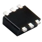
SC-89 Single (6 leads)
S
4
D
5
• TrenchFET® power MOSFET
APPLICATIONS
• Load switch for portable devices
D
1
D
Top View
2
D
3
G
G
Marking Code: D
N-Channel MOSFET
Ordering Information:
Si1078X-T1-GE3 (lead (Pb)-free and halogen-free)
S
ABSOLUTE MAXIMUM RATINGS (TA = 25 °C, unless otherwise noted)
PARAMETER
SYMBOL
LIMIT
Drain-Source Voltage
VDS
30
Gate-Source Voltage
VGS
± 12
TA = 25 °C
Continuous Drain Current (TJ = 150 °C) a
TA = 70 °C
Pulsed Drain Current (t = 100 μs)
Continuous Source-Drain Diode Current
TA = 25 °C
TA = 25 °C
Maximum Power Dissipation
TA = 70 °C
Operating Junction and Storage Temperature Range
UNIT
V
1.02 a, b
ID
0.82 a, b
IDM
6
IS
0.2 a, b
A
0.24 a, b
PD
W
0.15 a, b
TJ, Tstg
-55 to +150
°C
THERMAL RESISTANCE RATINGS
PARAMETER
Maximum Junction-to-Ambient a, c
SYMBOL
t5s
Steady State
RthJA
TYPICAL
MAXIMUM
440
530
540
650
UNIT
°C/W
Notes
a. Surface mounted on 1" x 1" FR4 board.
b. t = 5 s.
c. Maximum under steady state conditions is 650 °C/W.
S16-1056-Rev. A, 30-May-16
Document Number: 68549
1
For technical questions, contact: pmostechsupport@vishay.com
THIS DOCUMENT IS SUBJECT TO CHANGE WITHOUT NOTICE. THE PRODUCTS DESCRIBED HEREIN AND THIS DOCUMENT
ARE SUBJECT TO SPECIFIC DISCLAIMERS, SET FORTH AT www.vishay.com/doc?91000
�Si1078X
www.vishay.com
Vishay Siliconix
SPECIFICATIONS (TJ = 25 °C, unless otherwise noted)
PARAMETER
SYMBOL
TEST CONDITIONS
MIN.
TYP.
MAX.
UNIT
VDS
VGS = 0 V, ID = 250 μA
30
-
-
-
V
36.7
-
-
-2.8
-
Static
Drain-Source Breakdown Voltage
VDS/TJ
VDS Temperature Coefficient
VGS(th) Temperature Coefficient
VGS(th)/TJ
Gate-Source Threshold Voltage
VGS(th)
Gate-Source Leakage
IGSS
Zero Gate Voltage Drain Current
IDSS
On-State Drain Current a
ID(on)
Drain-Source On-State Resistance a
Forward Transconductance
ID = 250 μA
VDS = VGS, ID = 250 μA
0.6
-
1.5
VDS = 0 V, VGS = ± 12 V
-
-
± 20
VDS = 0 V, VGS = ± 4.5 V
-
-
±1
VDS = 30 V, VGS = 0 V
-
-
1
10
VDS = 30 V, VGS = 0 V, TJ = 85 °C
-
-
VDS = 5 V, VGS = 10 V
6
-
-
VGS = 10 V, ID = 1 A
-
0.118
0.142
VGS = 4.5 V, ID = 1 A
-
0.128
0.154
VGS = 2.5 V, ID = 0.5 A
-
0.150
0.195
VDS = 15 V, ID = 1 A
-
5.5
-
-
110
-
-
21
-
-
11
-
VDS = 15 V, VGS = 10 V, ID = 1 A
-
3
6
-
1.5
3
VDS = 15 V, VGS = 4.5 V, ID = 1 A
-
0.2
-
-
0.42
-
f = 1 MHz
1.04
5.2
5.6
-
8
16
-
25
38
-
23
35
tf
-
23
35
td(on)
-
5
10
-
23
35
-
10
20
-
35
53
RDS(on)
gfs
mV/°C
V
μA
A
S
Dynamic b
Input Capacitance
Ciss
Output Capacitance
Coss
Reverse Transfer Capacitance
Crss
Total Gate Charge
Qg
Gate-Source Charge
Qgs
Gate-Drain Charge
Qgd
Gate Resistance
Rg
Turn-On Delay Time
Rise Time
Turn-Off Delay Time
Fall Time
Turn-On Delay Time
Rise Time
Turn-Off Delay Time
Fall Time
VDS = 15 V, VGS = 0 V, f = 1 MHz
td(on)
tr
td(off)
tr
td(off)
VDD = 15 V, RL = 18.9
ID 0.8 A, VGEN = 4.5 V, Rg = 1
VDD = 15 V, RL = 18.9
ID 0.8 A, VGEN = 10 V, Rg = 1
tf
pF
nC
ns
Drain-Source Body Diode Characteristics
Pulse Diode Forward Current a
ISM
Body Diode Voltage
VSD
Body Diode Reverse Recovery Time
trr
Body Diode Reverse Recovery Charge
Qrr
Reverse Recovery Fall Time
ta
Reverse Recovery Rise Time
tb
IS = 0.8 A
IF = 2 A, dI/dt = 100 A/μs
-
-
6
-
0.75
1.2
A
V
-
12
20
ns
-
4
8
nC
-
7
-
-
5
-
ns
Notes
a. Pulse test; pulse width 100 μs, duty cycle 2 %.
b. Guaranteed by design, not subject to production testing.
Stresses beyond those listed under “Absolute Maximum Ratings” may cause permanent damage to the device. These are stress ratings only, and functional operation
of the device at these or any other conditions beyond those indicated in the operational sections of the specifications is not implied. Exposure to absolute maximum
rating conditions for extended periods may affect device reliability.
S16-1056-Rev. A, 30-May-16
Document Number: 68549
2
For technical questions, contact: pmostechsupport@vishay.com
THIS DOCUMENT IS SUBJECT TO CHANGE WITHOUT NOTICE. THE PRODUCTS DESCRIBED HEREIN AND THIS DOCUMENT
ARE SUBJECT TO SPECIFIC DISCLAIMERS, SET FORTH AT www.vishay.com/doc?91000
�Si1078X
www.vishay.com
Vishay Siliconix
TYPICAL CHARACTERISTICS (TA = 25 °C, unless otherwise noted)
Axis Title
Axis Title
10000
10-3
TJ = 25 °C
0.003
0.002
100
2nd line
IGSS - Gate Current (mA)
1000
0.004
1st line
2nd line
2nd line
IGSS - Gate Current (mA)
0.005
10000
10-4
1000
10-5
TJ = 150 °C
1st line
2nd line
0.006
10-6
100
TJ = 25 °C
10-7
0.001
0
10-8
10
0
3
6
9
12
10
0
15
3
6
9
12
15
VGS - Gate-to-Source Voltage (V)
2nd line
VGS - Gate-to-Source Voltage (V)
2nd line
Gate Current vs. Gate-to-Source Voltage
Gate Current vs. Gate-to-Source Voltage
Axis Title
Axis Title
6
10000
3
VGS = 10 V thru 3 V
3
VGS = 2 V
2
100
1
TC = 125 °C
1000
2
1.5
TC = 25 °C
TC = -55 °C
1
100
0.5
0
10
0
0.5
1
1.5
0
10
0
2
0.5
1
1.5
2
VDS - Drain-to-Source Voltage (V)
2nd line
VGS - Gate-to-Source Voltage (V)
2nd line
Output Characteristics
Transfer Characteristics
2.5
Axis Title
Axis Title
0.2
165
10000
10000
132
1000
0.14
VGS = 4.5 V
0.11
100
VGS = 10 V
0.08
Ciss
1000
99
1st line
2nd line
VGS = 2.5 V
2nd line
C - Capacitance (pF)
0.17
1st line
2nd line
2nd line
RDS(on) - On-Resistance (Ω)
1st line
2nd line
1000
4
2nd line
ID - Drain Current (A)
2.5
1st line
2nd line
2nd line
ID - Drain Current (A)
5
66
100
33
Coss
Crss
0.05
10
0
1.5
3
4.5
6
0
10
0
6
12
18
24
ID - Drain Current (A)
2nd line
VDS - Drain-to-Source Voltage (V)
2nd line
On-Resistance vs. Drain Current
Capacitance
S16-1056-Rev. A, 30-May-16
30
Document Number: 68549
3
For technical questions, contact: pmostechsupport@vishay.com
THIS DOCUMENT IS SUBJECT TO CHANGE WITHOUT NOTICE. THE PRODUCTS DESCRIBED HEREIN AND THIS DOCUMENT
ARE SUBJECT TO SPECIFIC DISCLAIMERS, SET FORTH AT www.vishay.com/doc?91000
�Si1078X
www.vishay.com
Vishay Siliconix
TYPICAL CHARACTERISTICS (TA = 25 °C, unless otherwise noted)
Axis Title
Axis Title
1.6
8
VDS = 15 V
1000
6
VDS = 24 V
4
100
2
0
1.4
1000
1.2
VGS = 2.5 V, 0.5 A
1.0
100
0.8
VGS = 4.5 V, 1 A
0.6
10
0
0.8
1.6
2.4
3.2
10
-50
-25
0
25
75
100 125 150
TJ - Junction Temperature (°C)
2nd line
Gate Charge
On-Resistance vs. Junction Temperature
Axis Title
Axis Title
0.25
1000
1st line
2nd line
TJ = 25 °C
0.1
100
0.01
0.001
0.2
TJ = 150 °C
0.4
0.6
0.8
1.0
1000
0.15
0.1
TJ = 25 °C
100
0.05
0
10
0.2
10000
1st line
2nd line
TJ = 150 °C
1
2nd line
RDS(on) - On-Resistance (Ω)
10000
10
2nd line
IS - Source Current (A)
50
Qg - Total Gate Charge (nC)
2nd line
100
0
10000
VGS = 10 V, Id=1 A
1st line
2nd line
VDS = 8 V
ID = 1 A
2nd line
RDS(on) - On-Resistance (Normalized)
10000
1st line
2nd line
2nd line
VGS - Gate-to-Source Voltage (V)
10
10
0
1.2
2
4
6
8
10
VSD - Source-to-Drain Voltage (V)
2nd line
VGS - Gate-to-Source Voltage (V)
2nd line
Source-Drain Diode Forward Voltage
On-Resistance vs. Gate-to-Source Voltage
Axis Title
5.0
10000
1.2
ID = 250 μA
4.0
0.8
Power (W)
1000
1st line
2nd line
2nd line
VGS(th) (V)
1.0
3.0
2.0
100
0.6
1.0
0.4
10
-50
-25
0
25
50
75
100 125 150
TJ - Temperature (°C)
2nd line
Threshold Voltage
S16-1056-Rev. A, 30-May-16
0
0.01
0.1
1
10
Time (s)
100
1000
Single Pulse Power, Junction-to-Ambient
Document Number: 68549
4
For technical questions, contact: pmostechsupport@vishay.com
THIS DOCUMENT IS SUBJECT TO CHANGE WITHOUT NOTICE. THE PRODUCTS DESCRIBED HEREIN AND THIS DOCUMENT
ARE SUBJECT TO SPECIFIC DISCLAIMERS, SET FORTH AT www.vishay.com/doc?91000
�Si1078X
www.vishay.com
Vishay Siliconix
TYPICAL CHARACTERISTICS (TA = 25 °C, unless otherwise noted)
Axis Title
10000
10
(1)
Limited
1 by RDS(on)
100 μs
1000
1 ms
1st line
2nd line
2nd line
ID - Drain Current (A)
IDM limited
10 ms
0.1
100 ms
0.01
100
DC, 10s, 1s
BVDSS limited
TA = 25 °C
Single pulse
0.001
10
0.1
(1)
1
10
100
VDS - Drain-to-Source Voltage (V)
VGS > minimum VGS at which RDS(on) is specified
Safe Operating Area, Junction-to-Ambient
Normalized Effective Transient
Thermal Impedance
1
Duty Cycle = 0.5
0.2
0.1
0.05
0.02
Notes:
0.1
PDM
t1
t2
1. Duty Cycle, D =
t1
t2
2. Per Unit Base = RthJA = 540 °C/W
3. TJM - TA = PDMZthJA(t)
Single Pulse
0.01
10-4
4. Surface Mounted
10-3
10-2
10-1
1
Square Wave Pulse Duration (s)
10
100
1000
Normalized Thermal Transient Impedance, Junction-to-Ambient
Vishay Siliconix maintains worldwide manufacturing capability. Products may be manufactured at one of several qualified locations. Reliability data for Silicon
Technology and Package Reliability represent a composite of all qualified locations. For related documents such as package/tape drawings, part marking, and
reliability data, see www.vishay.com/ppg?68549.
S16-1056-Rev. A, 30-May-16
Document Number: 68549
5
For technical questions, contact: pmostechsupport@vishay.com
THIS DOCUMENT IS SUBJECT TO CHANGE WITHOUT NOTICE. THE PRODUCTS DESCRIBED HEREIN AND THIS DOCUMENT
ARE SUBJECT TO SPECIFIC DISCLAIMERS, SET FORTH AT www.vishay.com/doc?91000
�Package Information
www.vishay.com
Vishay Siliconix
SC-89 6-Leads (SOT-563F)
E1/2
2
3
aaa
D
e1
4
C
2x
4
A
B
D
6
5
4
SECTION B-B
C
E/2
2
E
E1
3
6
2x
DETAIL “A”
aaa
C
1
5
2
2x
3
bbb
C
e
B
6x b
4
ddd
M
C
A–B D
L1
A1
L
A
A1
SEE DETAIL “A”
Notes
1. Dimensions in millimeters.
2. Dimension D does not include mold flash, protrusions or gate
burrs. Mold flush, protrusions or gate burrs shall not exceed
0.15 mm per dimension E1 does not include interlead flash
or protrusion, interlead flash or protrusion shall not exceed
0.15 mm per side.
3. Dimensions D and E1 are determined at the outmost extremes
of the plastic body exclusive of mold flash, the bar burrs, gate
burrs and interlead flash, but including any mismatch between
the top and the bottom of the plastic body.
4. Datums A, B and D to be determined 0.10 mm from the lead tip.
5. Terminal numbers are shown for reference only.
6. These dimensions apply to the flat section of the lead between
0.08 mm and 0.15 mm from the lead tip.
Revision: 11-Aug-14
DIM.
MILLIMETERS
MIN.
NOM.
A
0.56
0.58
MAX.
0.60
A1
0
0.02
0.10
b
0.15
0.22
0.30
0.18
c
0.10
0.14
D
1.50
1.60
1.70
E
1.50
1.60
1.70
1.25
E1
1.15
1.20
e
0.45
0.50
0.55
e1
0.95
1.00
1.05
L
0.25
0.35
0.50
L1
0.10
0.20
0.30
C14-0439-Rev. C, 11-Aug-14
DWG: 5880
Document Number: 71612
1
For technical questions, contact: analogswitchtechsupport@vishay.com
THIS DOCUMENT IS SUBJECT TO CHANGE WITHOUT NOTICE. THE PRODUCTS DESCRIBED HEREIN AND THIS DOCUMENT
ARE SUBJECT TO SPECIFIC DISCLAIMERS, SET FORTH AT www.vishay.com/doc?91000
�Application Note 826
Vishay Siliconix
RECOMMENDED MINIMUM PADS FOR SC-89: 6-Lead
0.051
0.012
0.020
(0.300)
(0.500)
0.019
(0.478)
0.031
(0.798)
0.069
(1.753)
(1.300)
0.051
(0.201)
Recommended Minimum Pads
Dimensions in Inches/(mm)
Return to Index
Return to Index
APPLICATION NOTE
Document Number: 72605
Revision: 21-Jan-08
www.vishay.com
21
�Legal Disclaimer Notice
www.vishay.com
Vishay
Disclaimer
ALL PRODUCT, PRODUCT SPECIFICATIONS AND DATA ARE SUBJECT TO CHANGE WITHOUT NOTICE TO IMPROVE
RELIABILITY, FUNCTION OR DESIGN OR OTHERWISE.
Vishay Intertechnology, Inc., its affiliates, agents, and employees, and all persons acting on its or their behalf (collectively,
“Vishay”), disclaim any and all liability for any errors, inaccuracies or incompleteness contained in any datasheet or in any other
disclosure relating to any product.
Vishay makes no warranty, representation or guarantee regarding the suitability of the products for any particular purpose or
the continuing production of any product. To the maximum extent permitted by applicable law, Vishay disclaims (i) any and all
liability arising out of the application or use of any product, (ii) any and all liability, including without limitation special,
consequential or incidental damages, and (iii) any and all implied warranties, including warranties of fitness for particular
purpose, non-infringement and merchantability.
Statements regarding the suitability of products for certain types of applications are based on Vishay's knowledge of typical
requirements that are often placed on Vishay products in generic applications. Such statements are not binding statements
about the suitability of products for a particular application. It is the customer's responsibility to validate that a particular product
with the properties described in the product specification is suitable for use in a particular application. Parameters provided in
datasheets and / or specifications may vary in different applications and performance may vary over time. All operating
parameters, including typical parameters, must be validated for each customer application by the customer's technical experts.
Product specifications do not expand or otherwise modify Vishay's terms and conditions of purchase, including but not limited
to the warranty expressed therein.
Hyperlinks included in this datasheet may direct users to third-party websites. These links are provided as a convenience and
for informational purposes only. Inclusion of these hyperlinks does not constitute an endorsement or an approval by Vishay of
any of the products, services or opinions of the corporation, organization or individual associated with the third-party website.
Vishay disclaims any and all liability and bears no responsibility for the accuracy, legality or content of the third-party website
or for that of subsequent links.
Except as expressly indicated in writing, Vishay products are not designed for use in medical, life-saving, or life-sustaining
applications or for any other application in which the failure of the Vishay product could result in personal injury or death.
Customers using or selling Vishay products not expressly indicated for use in such applications do so at their own risk. Please
contact authorized Vishay personnel to obtain written terms and conditions regarding products designed for such applications.
No license, express or implied, by estoppel or otherwise, to any intellectual property rights is granted by this document or by
any conduct of Vishay. Product names and markings noted herein may be trademarks of their respective owners.
© 2022 VISHAY INTERTECHNOLOGY, INC. ALL RIGHTS RESERVED
Revision: 01-Jan-2022
1
Document Number: 91000
�