TS2951
Taiwan Semiconductor
150mA Ultra Low Dropout Voltage Regulator
DESCRIPTION
FEATURES
The TS2951 are low power voltage regulators. These
●
Output voltage available in 5V, 3V & 3.3V
devices are excellent choice for use in battery-powered
●
Extremely low quiescent current
applications such as cordless telephone, radio control
●
Low dropout voltage
systems, and portable computers.
●
Extremely tight load and line regulation
The TS2951 is features very low quiescent current
●
Very low temperature coefficient
(75µA Typ.) and very low drop output voltage (Typ.
●
Need only 1µF for stability
40µV at light load and 380mV at 100mA). This includes
●
Use as Regulator or Reference
a tight initial tolerance of 1% (A version), extremely
●
Stable with low-ESR output capacitors
good load and line regulation 0.05% typ. and very low
●
Current and thermal limiting
output temperature coefficient, making the TS2951
●
Error Flag warns of output dropout
useful as a low-power voltage reference.
●
Logic-Controlled electronic shutdown
TS2951 have other key additional feature. The error flag
●
Additional voltage tap
output feature is used as power-on reset for warn of a
●
Output voltage sense
low output voltage, due to following batteries on input.
●
Output programmable from 1.24 to 29V
The logic-compatible shutdown input which enable the
APPLICATION
regulator to be switched on/off. The regulator output
●
Battery powered systems
voltage may be pin-strapped for a 5.0 & 3.3 & 3.0 of
●
SMPS Post-Regulator and Voltage Reference
programmed from 1.24V to 29V with external pair of
●
Voltage Reference
resistors. Using of as design, processing and testing
●
Portable consumer equipment
techniques
make
TS2951
superior
over
similar
products.
Pin Definition:
1. Output
2. Sense
3. Shutdown
4. Ground
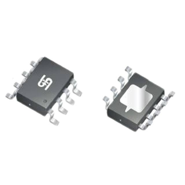
SOP-8
5.
6.
7.
8.
Error flag
Voltage tap
FB
Input
Notes: Moisture sensitivity level: level 3. Per J-STD-020
TYPICAL APPLICATION CIRCUIT
Adjustable Regulator
Document Number: DS_P0000207
1
Version: G15
�TS2951
Taiwan Semiconductor
ABSOLUTE MAXIMUM RATINGS
PARAMETER
SYMBOL
LIMIT
UNIT
Input Supply Voltage
VIN
-0.3 ~ +30
V
Feedback Input Voltage
VFB
-1.5 ~ +30
V
Shutdown Input Voltage
VSHUTDOWN
-0.3 ~ +30
V
VERROR
-0.3 ~ +30
V
PD
Internally Limited
Error Comparator Output Voltage
Power Dissipation
Operating Junction Temperature Range
TJ
TSTG
Storage Temperature Range
W
-40 ~ +125
o
-65 ~ +150
o
C
C
THERMAL PERFORMANCE
PARAMETER
SYMBOL
LIMIT
UNIT
Junction to Case Thermal Resistance
RӨJC
45
°C/W
Junction to Ambient Thermal Resistance
RӨJA
180
°C/W
Notes: RӨJA is the sum of the junction-to-case and case-to-ambient thermal resistances. The case thermal reference is defined
at the solder mounting surface of the drain pins. RӨJA is guaranteed by design while RӨCA is determined by the user’s board
design. RӨJA shown below for single device operation on FR-4 PCB in still air.
ELECTRICAL SPECIFICATIONS (VIN=VOUT+1V, TA=25oC, unless otherwise specified.)
CONDITIONS(Note 2)
PARAMETER
MIN
TYP
MAX
TJ=25 C
|0.985|
5.0
|1.015|
Full Operating temp
|0.980|
3.3
|1.020|
100uA≤ IL ≤100mA
|0.975|
3.0
|1.025|
--
50
150
--
20
100
--
0.04
0.2
%
--
0.1
0.3
%
50
80
mV
380
450
mV
75
120
µA
8
12
mA
o
Output Voltage
Output Voltage Temperature
Coefficient
(Note 1)
(Note 3)
Line Regulation
(Note 3)
Load Regulation
(Note 5)
Dropout Voltage
6V≤ VIN ≤30V
(Note 4)
100µA≤ IL ≤100mA
IL=100µA
--
IL=100mA
IL=100µA
Ground Current
--
IL=100mA
UNIT
V
o
ppm/ C
Dropout Ground Current
VIN= 4.5V, IL= 100uA
--
110
170
µA
Current Limit
VOUT= 0
--
160
200
mA
---
0.05
0.2
%W
430
--
CL= 3.3µF
--
100
--
CL= 200µF
--
160
--
1.21
1.235
1.27
V
1.185
1.235
1.285
V
Thermal Regulation
Output Noise, 10Hz to 100KHz
Bypass=0.01uF
CL= 1µF
µV/ rms
VREF ≤ VOUT ≤ (Vin-1V),
(Note 6)
Reference Voltage
2.3≤ Vin≤ 30V,
100uA≤ IL ≤ 100mA,
TJ ≤ TJ (max)
Document Number: DS_P0000207
2
Version: G15
�TS2951
Taiwan Semiconductor
ELECTRICAL SPECIFICATIONS (VIN=VOUT+1V, TA=25oC, unless otherwise specified.)
CONDITIONS(Note 2)
PARAMETER
MIN
TYP
MAX
UNIT
--
20
40
nA
--
20
--
ppm/ C
--
0.1
--
nA/ C
VOH= 30V
--
0.01
1
µA
VIN= 4.5V, IOL = 400µA
Feedback Pin Bias Current
Reference Voltage Temperature
(Note 7)
Coefficient
Feedback Pin Bias Current
Temperature Coefficient
Output Leakage Current
o
--
150
250
mV
(Note 8)
40
60
--
mV
(Note 8)
--
75
95
mV
--
15
--
mV
--
1.3
0.7
2.0
1.3
--
Vs = 2.4V
--
30
50
Vs = 30V
--
450
600
--
3
10
Output Low Voltage
Upper Threshold Voltage
Power Threshold Voltage
Hysteresis
o
(Note 8)
Output Logic Voltage
Shut down Pin Current
Low (Regulator ON)
High (Regulator OFF)
Regulator Output Current
shutdown
V
µA
µA
Note:
1. Output voltage temperature coefficients defined as the worst case voltage change divided by the total temperature range.
o
2. Unless otherwise specified all limits guaranteed for TJ= 25 C, VIN= 6V, IL= 100µA and CL= 100µF. Additional conditions for
the 8-pin versions are feedback tied to 5V, 3.3V & 3V tap output Sense (VOUT = 5V, 3.3V & 3V) and shutdown ≤ 0.8V.
3. Regulation is measured at constant junction temperature, using pulse testing with a low duty cycle. Changes in output
voltage due to heating effects are covered under the specification for thermal regulation.
o
o
4. Line regulation for the TS2951 is tested at 85 C for IL= 1mA. For IL= 100µA and TJ= 125 C, line regulation is guaranteed by
design to 0.2%.
5. Dropout Voltage is defined as the input to output differential at which the output voltage drops 100mV below its nominal
value measured at 1V differential at very low value of programmed output voltage, the minimum input supply voltage of 2V
(2.3V over temperature) must be taken in to account.
6. VREF ≤ VOUT ≤ (Vin-1V), 2.3≤ Vin≤ 30V, 100µA≤ IL ≤ 100mA, TJ ≤ TJ (max).
7. Reference voltage temperature coefficient is defined as the worst case voltage change divided by the total temperature
range.
8. Comparator thresholds are expressed in terms of a voltage differential at the feedback terminal below the nominal
reference voltage measured at 6V input. To express these thresholds in terms of output voltage change, multiply by the
error amplifier gain= VOUT / VREF = (R1+R2) / R2. For example, at a programmed output voltage of 5V, the Error output is
guaranteed to go low when the output drops by 95 mV X 5V / 1.250 = 384mV. Thresholds remain constant as a percent of
VOUT as VOUT is varied with the dropout warning occurring at typically 5% below nominal, 7.5% guaranteed.
Document Number: DS_P0000207
3
Version: G15
�TS2951
Taiwan Semiconductor
ORDERING INFORMATION
OUTPUT VOLTAGE
PACKAGE
PACKING
5.0V
TS2951CS50 RLG
PART NO.
SOP-8
2,500pcs / 13” Reel
3.3V
TS2951CS33 RLG
SOP-8
2,500pcs / 13” Reel
3.0V
TS2951CS30 RLG
SOP-8
2,500pcs / 13” Reel
Note:
1. Compliant to RoHS Directive 2011/65/EU and in accordance to WEEE 2002/96/EC.
2. Halogen-free according to IEC 61249-2-21 definition.
Document Number: DS_P0000207
4
Version: G15
�TS2951
Taiwan Semiconductor
BLOCK DIAGRAM
APPLICATION INFORMATION
External Capacitors
For the stability of the TS2951 is requires a 1.0µF (0.22µF is recommended for 3.0V & 3.3V) or greater capacitor
between output and ground. Oscillation could occur without this capacitor. The tantalum or aluminum electrolytic
o
works fine; could use the film type work but are not cost efficient. For the operation of below -25 C solid tantalum is
o
recommended since the many aluminum type have electrolytes the freeze at about -30 C. The ESR of about 5Ω or
less and resonant frequency above 500KHz are most important parameter in the value of Capacitor. The
Capacitors value can be increased without any limit. At lower values of output current, less output capacitance is
required for stability. For the currents below 10mA the value of capacitor can be reduce to 0.33µF and 0.1µF for
1mA. More output capacitance needed for the 8-pin version at voltage below 5V since it runs the error amplifier at
lower gain. At worst case 3.3≈F or greater must be used for condition of 100mA load at 1.250V output.
The TS2951 is not like other low dropout regulators will remain stable and regulation with no load in addition to the
internal voltage divider. This feature very important in application, it is like CMOS RAM keep-alive. The TS2951
output voltage is set with minimum load of 1µA and external resistors.
If at the input ofTS2951 connected to battery or between AC filter capacitor and input is 10 inches wire then 1uF
tantalum or aluminum electrolytic capacitor should be connected between input and ground. Instability can occur if
stray capacitor to feedback terminal pin 7 of the TS2951. This could cause more problems when using higher value
of external to set the output voltage. To fix this problem the 100pF capacitor between output and feedback and
increasing output capacitance to 3.3µF.
Document Number: DS_P0000207
5
Version: G15
�TS2951
Taiwan Semiconductor
APPLICATION INFORMATION (CONTINUE)
Reducing Output Noise
It could be an advantage to reduce the AC noise present at the output. One method is to reduce the regulator
bandwidth by increasing the value of the output capacitor. This is the only method that noise could reduce on the
TS2951, but is relatively inefficient, as increasing capacitor from 1µF to 220µF only decreases the noise from
430µV to 160µVrms for a 100KHz bandwidth at 5V output. Noise could be also reduced by fourfold by a bypass
capacitor across R1 since it reduces the high frequency gain from 4 to unity.
Pick Cbypass= 1 / 2πR1 * 200Hz or choose 0.01µF when doing this, the output capacitor must be increased to
3.3uF to maintain stability. These change the output noise from 430µV/rms for a 100 kHz bandwidth 5V, 3.3V & 3V
output. With the bypass capacitor added, noise no longer scales with output voltage so that improvements are
more dramatic higher output voltage.
Error Detection Comparator Output
The Compactor produces a logic low output whenever the TS2951 output falls of regulation by more than around
5%. This is around 60 mV offset divided by the 1.235 reference voltage. Thus trip remains 5% below nominal
regardless of the programmed output voltage of the regulator. The Figure 1 shows the timing diagram depicting the
ERROR signal and the regulator output voltage as the TS2951 input is ramped up and down. The ERROR signal
becomes low at around 1.3V input, it goes high around 5V input (input voltage at which VOUT=4.75V). The TS2951
dropout voltage depending on the load, the input voltage trip point around 5V will vary with load current. The output
voltage trip point is around 4.75V, it does not change with load. The error comparator has an open-collector output
which requires an external pull-up resistor. Depending on the system requirement, the resistor maybe returned to 5
or 3.3V output or other supply voltage depending to the system requirements. For determining the size of the
resistor, note that the output is sinking 400uA, this value adds to battery drain in a low better condition,
recommended values 100K to 1MΩ. If the output is unused this resistor is not required.
Programming The output Voltage
The TS2951 output voltage is programmable for any value from it reference voltage of 1.235V and it maximum
rating of 30V. For example for 5 volt needs to pin-strapped and using the internal voltage divider by tying pin 1 to 2
and pin 7 to pin 6. There are two external resistor required for this programming. Refer to the below equation for
the programming the output voltage:
Volt=VREF x (1+R1\R2)+IFB * R1
The VREF is 1.235V and IFB is the feedback bias current, nominally -20nA. The minimum recommended load current
of 1µA forces an upper limit of 1.2MΩon value of R2, If no load presented the IFB produces error of typically 2% in
VOUT which maybe eliminated at room temperature by trimming R1. To improve the accuracy chooses the value of
R2=100K and this reduces the error by 0.17% and increases the resistor program current by 12µA. The TS2951
typically draw 60µA at no load with pin 2 open-circuit, and this value does not look much.
Error Output Timing
Document Number: DS_P0000207
6
Version: G15
�TS2951
Taiwan Semiconductor
CHARACTERISTICS CURVES
(TA = 25°C unless otherwise noted)
Figure 1. Line Regulation vs. Input Voltage
Figure 2. Load Regulation vs. Output Current
Figure 3. Ground Pin Current vs. Output Current Figure 4. Ground Pin Current vs. Input Voltage
Figure 5. Dropout Voltage vs. Output Current
Document Number: DS_P0000207
Figure 6. Load Transient Response
7
Version: G15
�TS2951
Taiwan Semiconductor
PACKAGE OUTLINE DIMENSIONS (Unit: Millimeters)
SOP-8
SUGGESTED PAD LAYOUT (Unit: Millimeters)
MARKING DIAGRAM
XX
= Voltage Code
(50=5.0V, 33=3.3V, 30=3.0V )
Y
M
= Year Code
= Month Code for Halogen Free Product
O =Jan P =Feb Q =Mar R =Apr
S =May T =Jun U =Jul
V =Aug
W =Sep X =Oct
Y =Nov Z =Dec
= Lot Code
L
Document Number: DS_P0000207
8
Version: G15
�TS2951
Taiwan Semiconductor
Notice
Specifications of the products displayed herein are subject to change without notice. TSC or anyone on its behalf,
assumes no responsibility or liability for any errors or inaccuracies.
Information contained herein is intended to provide a product description only. No license, express or implied, to
any intellectual property rights is granted by this document. Except as provided in TSC’s terms and conditions of
sale for such products, TSC assumes no liability whatsoever, and disclaims any express or implied warranty,
relating to sale and/or use of TSC products including liability or warranties relating to fitness for a particular purpose,
merchantability, or infringement of any patent, copyright, or other intellectual property right.
The products shown herein are not designed for use in medical, life-saving, or life-sustaining applications.
Customers using or selling these products for use in such applications do so at their own risk and agree to fully
indemnify TSC for any damages resulting from such improper use or sale.
Document Number: DS_P0000207
9
Version: G15
�


 工商网监
湘ICP备2023018690号
工商网监
湘ICP备2023018690号
