CGHV35060MP
60 W, 2700-3800 MHz, 50 V GaN HEMT for
S Band Radar and LTE Base Stations
Description
CGHV35060MP is a 60 W input matched, gallium nitride (GaN) high electron
mobility transistor (HEMT) optimized for S Band performance. The
CGHV35060MP is suitable for typical bands of 2.7-3.1 GHz and 3.1-3.5 GHz while
the input matched transistor provides optimal gain, power and efficiency in
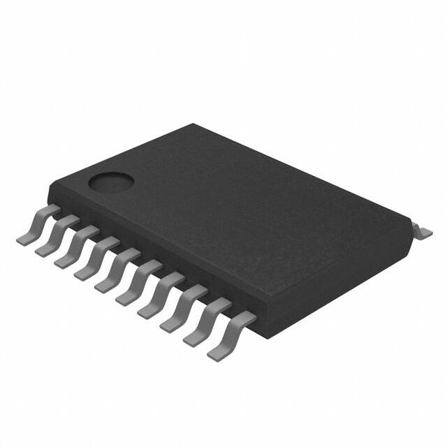
a small 6.5 mm x 4.4 mm plastic surface mount (SMT) package. The typical
performance plots in the datasheet are derived with CGHV35060MP matched
into a 3.1-3.5 GHz high power amplifier.
PN: CGHV35060MP
Typical Performance Over 3.1 - 3.5 GHz (TC = 25˚C) of Demonstration Amplifier
Parameter
3.1 GHz
3.3 GHz
3.5 GHz
Units
Gain
14.5
14.3
13.8
dB
Output Power
88
88
75
W
Drain Efficiency
61
67
64
%
Note: Measured in the CGHV35060MP-AMP1 amplifier circuit, under 100 μs pulse width, 10% duty cycle, PIN = 35 dBm
Features
•
•
•
•
•
Reference design amplifier 3.1 - 3.5 GHz
75W Typical output power
14.5 dB power gain
67% Drain efficiency
Internally pre-matched on input, unmatched output
Large Signal Models Available for ADS and MWO
Rev 2.3 - July 2021
4600 Silicon Drive | Durham, NC 27703 | wolfspeed.com
�CGHV35060MP
2
Absolute Maximum Ratings (not simultaneous) at 25˚C Case Temperature
Parameter
Symbol
Rating
Units
Conditions
Drain-Source Voltage
VDSS
150
Volts
25˚C
Gate-to-Source Voltage
VGS
-10, +2
Volts
25˚C
Storage Temperature
TSTG
-65, +150
˚C
Operating Junction Temperature
TJ
225
˚C
Maximum Forward Gate Current
IGMAX
10.4
mA
25˚C
Maximum Drain Current1
IDMAX
6.3
A
25˚C
Soldering Temperature2
TS
245
˚C
CW Thermal Resistance, Junction to Case3
RθJC
2.6
˚C/W
85˚C, PDISS = 52 W
Pulsed Thermal Resistance, Junction to Case
RθJC
1.95
˚C/W
85˚C, PDISS = 62 W, 100 μsec 10%
Case Operating Temperature4
TC
-40, +107
˚C
CW
Notes:
1
Current limit for long term, reliable operation
2
Refer to the Application Note on soldering at wolfspeed.com/rf/document-library
3
Measured for the CGHV35060MP
4
See also, the Power Dissipation De-rating Curve on Page 4
Electrical Characteristics (TC = 25˚C)
Characteristics
Symbol Min.
Typ.
Max.
Units
Conditions
Gate Threshold Voltage
VGS(th)
-3.8
-3.0
-2.3
VDC
VDS = 10 V, ID = 10.4 mA
Gate Quiescent Voltage
VGS(Q)
–
-2.7
–
VDC
VDS = 50 V, ID = 125 mA
Saturated Drain Current2
IDS
8.4
10.4
–
A
VDS = 6.0 V, VGS = 2.0 V
Drain-Source Breakdown Voltage
VBR
125
–
–
VDC
VGS = -8 V, ID = 10.4 mA
DC Characteristics
1
RF Characteristics (TC = 25˚C, F0 = 3.225 GHz unless otherwise noted)
4
Saturated Output Power3,6
PSAT
55
75
–
W
VDD = 50 V, IDQ = 125 mA, PIN = 34.5 dBm
Pulsed Drain Efficiency
η
46
59.1
–
%
VDD = 50 V, IDQ = 125 mA, PIN = 34.5 dBm
Gain3,6
G
14.35
16.3
–
dB
VDD = 50 V, IDQ = 125 mA, PIN = 10 dBm
Output Mismatch Stress3
VSWR
–
–
10:1
Y
No damage at all phase angles,
VDD = 50 V, IDQ = 125 mA, POUT = 60 W Pulsed
CGS
–
32.16
–
pF
VDS = 50 V, Vgs = -8 V, f = 1 MHz
Output Capacitance
CDS
–
4.4
–
pF
VDS = 50 V, Vgs = -8 V, f = 1 MHz
Feedback Capacitance
CGD
–
0.5
–
pF
VDS = 50 V, Vgs = -8 V, f = 1 MHz
3,6
Dynamic Characteristics
Input Capacitance5
5
Notes:
1
Measured on wafer prior to packaging
2
Scaled from PCM data
3
Pulse Width = 100 μs, Duty Cycle = 10%
4
Measured in CGHV35060MP high volume test fixture
5
Includes package
6
Includes offsets correlating data taken in high volume test fixture to data taken in application circuit with device soldered down
Rev 2.3 - July 2021
4600 Silicon Drive | Durham, NC 27703 | wolfspeed.com
�CGHV35060MP
3
Typical Performance
Figure 1. Small Signal Gain and Return Losses vs Frequency
Measured in Demonstration Amplifier
Circuit CGHV35060MP-AMP1
CGHV35060MP
35dBm pin, 10% 100us, Vd 50V, Id 125mA
20
10
Gain and Return Loss (dB)
Gain and Return Loss (dB)
15
5
0
-5
-10
S21
-15
S11
S22
-20
2.8
2.9
3.0
3.1
3.2
3.3
3.4
Frequency (GHz)
3.5
3.6
3.7
3.8
Frequency (GHz)
Figure 2. Gain, Efficiency & Output Power vs Frequency
mA, Pulse Width = 100 us, Duty Cycle = 10%, Tcase = 25°C
VDD = 50 V IDQ = 125
Figure 2. CGHV35060MP Output Power vs. Input Power
Vdd = 50V IDQ = 125mA, Pulse Width = 100us, Duty Cycle = 10%, Tcase = 25°C
105
40
95
35
Output Power
90
30
85
80
25
Efficiency
70
20
65
Gain
60
55
15
50
45
Power
40
Efficiency
35
Gain
Power Gain (dB)
75
Power Gain (dB)
Power (W) and Drain Efficiency (%)
Power (W) and Drain Efficiency (%)
100
10
5
30
25
3.1
3.2
3.3
Input Power (dBm)
3.4
3.5
0
Frequency (GHz)
Rev 2.3 - July 2021
4600 Silicon Drive | Durham, NC 27703 | wolfspeed.com
�CGHV35060MP
4
Typical Performance
Figure 3. CGHV35060MP-AMP1 Output Power vs. Input Power
VDD = 50 V IDQ = 125
mA,3. Pulse
WidthOutput
= 100Power
us, Duty
Cycle
Figure
CGHV35060MP
vs. Input
Power= 10%, Tcase = 25°C
Vdd = 50V IDQ = 125mA, Pulse Width = 100us, Duty Cycle = 10%, Tcase = 25°C
52
48
Output Power (dBm)
Output Power (dBm)
50
46
Pout 3.1 GHz
44
Pout 3.2 GHz
42
Pout 3.3 GHz
Pout 3.4 GHz
40
Pout 3.5 GHz
38
21
22
23
24
25
26
27
28
29
Input Power (dBm)
30
31
32
33
34
35
Input Power (dBm)
Figure 4. CGHV35060MP-AMP1 Gain & Efficiency vs Input Power
mA, 4.Pulse
Width = 100 us, Duty Cycle = 10%, Tcase = 25°C
VDD = 50 V IDQ = 125Figure
CGHV35060MP Output Power vs. Input Power
65
19
60
18
55
17
50
16
45
15
40
14
35
13
30
12
25
20
15
10
Gain (dB)
20
Gain (dB)
Drain Efficiency (%)
Drain Efficiency (%)
Vdd = 50V IDQ = 125mA, Pulse Width = 100us, Duty Cycle = 10%, Tcase = 25°C
70
21
22
23
24
25
26
27
28
29
Input Power (dBm)
DEff 3.1 GHz
DEff 3.2 GHz
DEff 3.3 GHz
DEff 3.4 GHz
DEff 3.5 GHz
Gain 3.1 GHz
Gain 3.2 GHz
Gain 3.3 GHz
Gain 3.4 GHz
Gain 3.5 GHz
30
31
32
33
34
11
10
9
35
8
Input Power (dBm)
Rev 2.3 - July 2021
4600 Silicon Drive | Durham, NC 27703 | wolfspeed.com
�CGHV35060MP
5
Typical Performance
Figure 5. CGHV35060MP-AMP1 Tj_rise vs. Input Power
VDD = 50 V IDQ = 125 mA, Pulse Width = 100 us, Duty Cycle = 10%, Tcase = 25°C
Tj_rise (°C)
Tj_rise (°C)
Figure 5. CGHV35060MP Tj_rise vs. Input Power
Vdd = 50V IDQ = 125mA, Pulse Width = 100us, Duty Cycle = 10%, Tcase = 25°C
125
120
115
110
105
100
95
90
85
80
75
70
65
60
55
50
45
40
35
30
25
20
15
10
5
0
T_rise 3.1 GHz
T_rise 3.2 GHz
T_rise 3.3 GHz
T_rise 3.4 GHz
T_rise 3.5 GHz
21
22
23
24
25
26
27
28
29
Input Power (dBm)
30
31
32
33
34
35
Input Power (dBm)
Figure 6. CGHV35060MP-AMP1 Output Power vs. Time, Varying Pulse Lengths
VDD = 50 V PINOutput
= 35 dBm,
Duty Cycle = 10%
Figure 6. - CGHV35060MP
Power vs. Time, Varying Pulse Lengths
Vdd = 50V, PIN = 35 dBm, Duty Cycle = 10%
50.0
100us
200us
49.5
300us
500uS
Power (dBm)
Power (dBm)
49.0
48.5
48.0
47.5
47.0
0
50
100
150
200
250
300
Time (us)
350
400
450
500
550
600
Time (us)
Rev 2.3 - July 2021
4600 Silicon Drive | Durham, NC 27703 | wolfspeed.com
�CGHV35060MP
6
CGHV35060MP Power Dissipation De-rating Curve
Power dissipation derating curve vs. Max Tcase
Pulsed (100 uS/ 10% duty)
100
90
Power Dissipation (W)
80
Power dissipation (W)
70
60
50
Note 1
40
30
20
Pulse 100uS / 10%
10
0
0
50
100
150
200
250
Case Temperature (C)
Case Temperature (C)
Note 1. Area exceeds Maximum Case Temperature (See Page 2)
CGHV35060MP-AMP1 Application Circuit Bill of Materials
Designator
Description
Qty
R1
RES,1/16W,0603,1%,150 OHMS
1
R20,R21
RES,1/16W,0603,1%,10.0 OHMS
2
C1
CAP, 2.2pF, +/-0.1pF, 0603, ATC
1
C2,C20-C30
CAP, 10.0pF, +/-5%, 0603, ATC
12
C3,C4
CAP, 1.3pF, +/-0.1pF, 0603, ATC
2
C11,C14
CAP, 0.7pF, +/-0.05pF, 0603, ATC
2
C13,C12
CAP, 0.9pF, +/-0.05 pF, 0603, ATC
2
C15,C16
CAP, 1.0pF, +/-0.05pF, 0603, ATC
2
C17
CAP, 0.1pF, +/-0.05pF, 0603, ATC
1
C41,C42,C43
CAP CER 2.2UF 100V 10% X7R 1210
3
C51,C53
CAP CER 10UF 100V 20% X7S 2220
2
C61
CAP, 33 UF, 20%, G CASE, 100V
1
J1,J2
SMA PANEL RECEPTACLE JACK
2
J3
HEADER RT>PLZ .1CEN LK 5POS
1
Cu BASEPLATE 2.6 x 1.7 x 0.25” WITH PEDESTAL FOR GULLWING eTSSOP
1
PCB, TEST FIXTURE, RO4350, .020 THK, CGHV35060MP
1
2-56 SOC HD SCREW 1/4 SS
4
#2 SPLIT LOCKWASHER SS
4
PREFORM, eTSSOP, 0.174 x 0.130 x 0.005
1
60W, GaN HEMT TSSOP 20L, 2.7 -3.5GHz, 50V PLASTIC, "CGHV35060MP"
1
Q1
Rev 2.3 - July 2021
4600 Silicon Drive | Durham, NC 27703 | wolfspeed.com
�CGHV35060MP
7
CGHV35060MP-AMP1 Application Circuit Outline
CGHV35060MP-AMP1 Application Circuit Schematic
Rev 2.3 - July 2021
4600 Silicon Drive | Durham, NC 27703 | wolfspeed.com
�CGHV35060MP
8
Product Dimensions CGHV35060MP (4.4 mm TSSOP 20-Lead Package)
Rev 2.3 - July 2021
4600 Silicon Drive | Durham, NC 27703 | wolfspeed.com
�CGHV35060MP
9
Part Number System
CGHV35060MP
Plastic Overmold
Power Output (W)
Upper Frequency (GHz)
Cree GaN High Voltage
Table 1.
Parameter
Value
Units
Upper Frequency1
3.5
GHz
Power Output
60
W
Package
MP
-
Note1: Alpha characters used in frequency code indicate a value
greater than 9.9 GHz. See Table 2 for value.
Table 2.
Rev 2.3 - July 2021
Character Code
Code Value
A
0
B
1
C
2
D
3
E
4
F
5
G
6
H
7
J
8
K
9
Examples:
1A = 10.0 GHz
2H = 27.0 GHz
4600 Silicon Drive | Durham, NC 27703 | wolfspeed.com
�CGHV35060MP
10
Product Ordering Information
Order Number
Description
Unit of Measure
CGHV35060MP
GaN HEMT
Each
CGHV35060MP-AMP1
Test board with GaN HEMT installed
Each
Rev 2.3 - July 2021
Image
4600 Silicon Drive | Durham, NC 27703 | wolfspeed.com
�CGHV35060MP
11
For more information, please contact:
4600 Silicon Drive
Durham, North Carolina, USA 27703
www.wolfspeed.com/rf
Sales Contact
rfsales@cree.com
Notes & Disclaimer
Specifications are subject to change without notice. “Typical” parameters are the average values expected by Cree
in large quantities and are provided for information purposes only. Cree products are not warranted or authorized
for use as critical components in medical, life-saving, or life-sustaining applications, or other applications where
a failure would reasonably be expected to cause severe personal injury or death. No responsibility is assumed by
Cree for any infringement of patents or other rights of third parties which may result from use of the information
contained herein. No license is granted by implication or otherwise under any patent or patent rights of Cree.
© 2014 – 2021 Cree, Inc. All rights reserved. Wolfspeed® and the Wolfspeed logo are registered trademarks of Cree, Inc.
Rev 2.3 - July 2021
4600 Silicon Drive | Durham, NC 27703 | wolfspeed.com
�