AO3402
N-Channel30-V(D-S)MOSFET
V(BR)DSS
RDS(on)MAX
ID
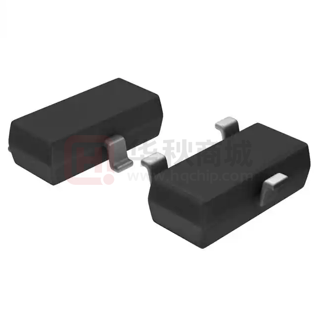
SOT-23
0.055Ω@ 10V
3
30V
1.GATE
4.0 A
0.070Ω@ 4.5V
2.SOURCE
0.100Ω@ 2.5V
3.DRAIN
JS
1
2
MI
General FEATURE
Equivalent Circuit
CR
●TrenchFET Power MOSFET
●Lead free product is acquired
O
●Surface mount package
co
mi
Se
APPLICATION
●Load Switch for Portable Devices
●DC/DC Converter
TA=25°C
Pulsed Drain Current
Power Dissipation
A
B
TA=25°C
Junction and Storage Temperature Range
Thermal Characteristics
Parameter
Maximum Junction-to-Ambient
Maximum Junction-to-Ambient
C
Maximum Junction-to-Lead
Maximum
30
Units
V
±12
V
ID
4
A
IDM
15
PD
1.25
TJ, TSTG
A
t ≤ 10s
Steady-State
Steady-State
W
°C
-55 to 150
Symbol
A
r
to
uc
Continuous Drain
Current A
nd
Absolute Maximum Ratings TA=25°C unless otherwise noted
Parameter
Symbol
VDS
Drain-Source Voltage
VGS
Gate-Source Voltage
RθJA
RθJL
Typ
70
100
63
www.jsmsemi.com
Max
90
125
80
Units
°C/W
°C/W
°C/W
第1/5页
�AO3402
N-Channel30-V(D-S)MOSFET
Electrical Characteristics (TJ=25°C unless otherwise noted)
Min
ID=250µA, VGS=0V
30
IDSS
Zero Gate Voltage Drain Current
VDS=24V, VGS=0V
1
µA
IGSS
VGS(th)
Gate-Body leakage current
VDS=0V, VGS=±12V
100
nA
Gate Threshold Voltage
1.2
On state drain current
JS
VDS=VGS ID=250µA
VGS=4.5V, VDS=5V
0.8
ID(ON)
V
A
VGS=10V, ID=4A
50
55
mΩ
RDS(ON)
Static Drain-Source On-Resistance
VGS=4.5V, ID=2.3A
65
70
90
8
0.8
100
gFS
VSD
VGS=2.5V, ID=1.5A
Forward Transconductance
VDS=5V, ID=4A
Diode Forward Voltage
IS=1A,VGS=0V
Maximum Body-Diode Continuous Current
mΩ
mΩ
1.2
2.5
S
V
A
Symbol
Gate resistance
SWITCHING PARAMETERS
Qg
Total Gate Charge
Qgs
Gate Source Charge
4.34
0.6
1.38
nC
nC
nC
3.3
1
ns
ns
VGS=4.5V, VDS=15V, ID=4A
Gate Drain Charge
Turn-On DelayTime
Turn-On Rise Time
Turn-Off DelayTime
Turn-Off Fall Time
VGS=10V, VDS=15V, RL=3.75Ω,
RGEN=6Ω
Body Diode Reverse Recovery Time
IF=4A, dI/dt=100A/µs
Body Diode Reverse Recovery Charge IF=4A, dI/dt=100A/µs
r
to
uc
Qrr
VGS=0V, VDS=0V, f=1MHz
pF
pF
pF
Ω
nd
tf
trr
V
co
Rg
Units
390
54.5
41
3
VGS=0V, VDS=15V, f=1MHz
mi
Output Capacitance
Reverse Transfer Capacitance
Max
10
Se
Coss
Crss
tD(off)
Typ
O
DYNAMIC PARAMETERS
Ciss
Input Capacitance
Qgd
tD(on)
tr
0.6
CR
IS
Parameter
MI
Conditions
STATIC PARAMETERS
BVDSS
Drain-Source Breakdown Voltage
21.7
2.1
12
ns
ns
ns
nC
6.3
A: The value of R θJA is measured with the device mounted on 1in2 FR-4 board with 2oz. Copper, in a still air environment with TA =25°C. The
value in any a given application depends on the user's specific board design. The current rating is based on the t ≤ 10s thermal resistance
rating.
B: Repetitive rating, pulse width limited by junction temperature.
C. The R θJA is the sum of the thermal impedence from junction to lead RθJL and lead to ambient.
D. The static characteristics in Figures 1 to 6,12,14 are obtained using 80 µs pulses, duty cycle 0.5% max.
E. These tests are performed with the device mounted on 1 in 2 FR-4 board with 2oz. Copper, in a still air environment with TA=25°C. The
SOA curve provides a single pulse rating.
www.jsmsemi.com
第2/5页
�AO3402
N-Channel30-V(D-S)MOSFET
TYPICAL ELECTRICAL AND THERMAL CHARACTERISTICS
10
15
10V
3V
12
8
VDS=5V
4.5V
6
ID(A)
ID (A)
9
2.5V
6
4
125°C
JS
3
MI
0
0
1
2
VGS=2V
2
25°C
0
3
4
5
0
0.5
CR
O
150
90
VGS=4.5V
60
30
1.6
2.5
3
3.5
VGS=4.5V
VGS=10V
1.4
1.2
VGS=2.5V
1
co
VGS=10V
0
0.8
0
2
4
6
8
10
0
25
75
100
125
150
175
Temperature (°C)
Figure 4: On-Resistance vs. Junction
Temperature
r
to
uc
200
1.0E+01
1.0E+00
150
50
nd
ID (A)
Figure 3: On-Resistance vs. Drain Current and
Gate Voltage
ID=2A
1.0E-01
125°C
100
IS (A)
RDS(ON) (mΩ)
2
mi
Se
RDS(ON) (mΩ)
VGS=2.5V
120
1.5
1.8
Normalized On-Resistance
180
1
VGS(Volts)
Figure 2: Transfer Characteristics
VDS (Volts)
Fig 1: On-Region Characteristics
125°C
1.0E-02
1.0E-03
25°C
1.0E-04
50
25°C
1.0E-05
1.0E-06
0
0
2
4
6
8
10
VGS (Volts)
Figure 5: On-Resistance vs. Gate-Source Voltage
0.0
0.2
0.4
0.6
0.8
1.0
1.2
VSD (Volts)
Figure 6: Body-Diode Characteristics
www.jsmsemi.com
第3/5页
�AO3402
N-Channel30-V(D-S)MOSFET
TYPICAL ELECTRICAL AND THERMAL CHARACTERISTICS
600
5
VDS=15V
ID=4A
500
Capacitance (pF)
VGS (Volts)
4
3
2
JS
1
0
1
300
200
Coss
100
MI
0
Ciss
400
2
0
3
4
5
0
Qg (nC)
Figure 7: Gate-Charge Characteristics
0.1s 10ms
1.0
1s
10
1
10
100
0
0.001
1
10
100
1000
r
to
uc
ZθJA Normalized Transient
Thermal Resistance
0.1
Pulse Width (s)
Figure 10: Single Pulse Power Rating Junction-toAmbient (Note E)
Figure 9: Maximum Forward Biased Safe
Operating Area (Note E)
D=Ton/T
TJ,PK=TA+PDM.ZθJA.RθJA
RθJA=90°C/W
0.01
nd
VDS (Volts)
co
DC
0.1
10
30
5
10s
0.1
25
15
10µs
Power (W)
1ms
20
mi
ID (Amps)
100µs
15
TJ(Max)=150°C
TA=25°C
Se
RDS(ON)
limited
10
20
O
10.0
5
VDS (Volts)
Figure 8: Capacitance Characteristics
CR
TJ(Max)=150°C
TA=25°C
100.0
Crss
In descending order
D=0.5, 0.3, 0.1, 0.05, 0.02, 0.01, single pulse
1
PD
0.1
Ton
T
Single Pulse
0.01
0.00001
0.0001
0.001
0.01
0.1
1
10
100
1000
Pulse Width (s)
Figure 11: Normalized Maximum Transient Thermal Impedance
www.jsmsemi.com
第4/5页
�AO3402
N-Channel30-V(D-S)MOSFET
SOT-23 Package Outline Dimensions
JS
MI
Se
co
www.jsmsemi.com
r
to
uc
nd
SOT-23 Suggested Pad Layout
Dimensions In Inches
Min
Max
0.035
0.045
0.000
0.004
0.035
0.041
0.012
0.020
0.003
0.006
0.110
0.118
0.047
0.055
0.089
0.100
0.037 TYP
0.071
0.079
0.022 REF
0.012
0.020
0°
8°
mi
Dimensions In Millimeters
Min
Max
0.900
1.150
0.000
0.100
0.900
1.050
0.300
0.500
0.080
0.150
2.800
3.000
1.200
1.400
2.250
2.550
0.950 TYP
1.800
2.000
0.550 REF
0.300
0.500
0°
8°
O
A
A1
A2
b
c
D
E
E1
e
e1
L
L1
θ
CR
Symbol
第5/5页
�
很抱歉,暂时无法提供与“AO3402”相匹配的价格&库存,您可以联系我们找货
免费人工找货- 国内价格
- 1+0.10260
- 100+0.09576
- 300+0.08892
- 500+0.08208
- 2000+0.07866
- 5000+0.07661


 工商网监
湘ICP备2023018690号
工商网监
湘ICP备2023018690号
