TVS Diode Arrays (SPA®® Diodes)
SRV05-4HTG-D, 5V 10A TVS Diode Array
RoHS
Pb GREEN
Description
The SRV05-4HTG-D integrates low capacitance rail-torail diodes with an additional zener diode to protect each
I/O pin against ESD and high surge events. This robust
device can safely absorb 10A surge current per
IEC61000-45 (tP=8/20μs) without performance degradation and a
minimum ±30kV ESD per IEC 61000-4-2. Their very low
loading capacitance also makes them ideal for
protecting high speed signal pins.
Features
Pinout
I/O 1
I/O 4
• Low leakage current of
0.5μA (MAX) at 5V
• EFT, IEC61000-4-4, 40A
(5/50ns)
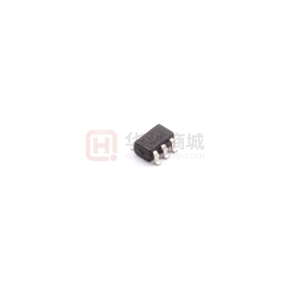
• Small SOT23-6 (JEDEC
MO-178) packaging
• Lightning, 10A (8/20μs as
defined in IEC 61000-4-5
2nd edition)
• Halogen free, lead free
and RoHS compliant
• Low capacitance of 1pF
(TYP) per I/O
VCC
GND
• ESD, IEC 61000-4-2,
±30kV contact, ±30kV air
• Moisture Sensitivity Level
(MSL -1)
Applications
Top View
• Monitors
• Set Top Boxes
• Notebooks
• Flat Panel Displays
TX +
SP3003-04J/XTG
5
• Firewire
Ethernet Differential
Protection
• Portable
Medical
• 10/100/100010/100
Ethernet
Functional Block Diagram
6
• LCD/PDP TVs
4
Application Examples
Unused
TX +
SP3003-04ATG
USB Dual Port Protection
10
10/100
Ethernet
9 PHY 8
7
6
RT
TX -
USB
Controller
RX +
RT
TX -
VBUS
1
6
2
5
VBUS
3
4
D+
DGND
SRV05-4HTG-D
SRV05-4HTG
CT
75
75
75 V
GND
RT
CT
1
2
3
1
2
3
D+
D-
5
4
5
SP3003-08ATG
8
910/100/1000
Ethernet
PHY
7
TX -
Unused
TX +
6
TX -
1
6
2
5
3
4
SRV05-4HTG-D
SRV05-4HTG
RX +
RJ45
Unused
TX +
10
USB
Port
GND
10/100/1000 Ethernet Protection
SP3003-02J/XTG
75
VBUS
CT
4
Unused
BUS
VCC
RT
RX -
Unused
RX VCC
USB
Port
RX +
SRV05-4HTG
VBUS
CT
RJ45
Unused
RX +
RX Unused
Unused
Life Support Note:
Not Intended for Use in Life Support or Life Saving Applications
RX VCC
The products shown herein are not designed for use in life sustaining or life saving
applications unless otherwise expressly indicated.
VCC
GND
©2019 Littelfuse, Inc.
1
2
Specifications are subject to change without notice.
Revision: 03/18/19
3
1
2
3
4
To Twisted-Pair Network
I/O 3
5
To Twisted-Pair Network
I/O 2
�TVS Diode Arrays (SPA®® Diodes)
Low Capacitance ESD Protection - SRV05-4HTG-D
Absolute Maximum Ratings
Symbol
Parameter
Value
Units
IPP
Peak Current (tp=8/20μs)
10
A
PPk
Peak Pulse Power (tp=8/20μs)
150
W
TOP
Operating Temperature
-40 to 125
°C
TSTOR
Storage Temperature
-55 to 150
°C
Notes:
CAUTION: Stresses above those listed in “Absolute Maximum Ratings” may cause permanent damage to the component. This is a stress only rating and
operation of the component at these or any other conditions above those indicated in the operational sections of this specification is not implied.
Electrical Characteristics (TOP=25ºC)
Parameter
Symbol
Test Conditions
Reverse Standoff Voltage
VRWM
IR = 1μA, I/O to GND
Breakdown Voltage
VBR
IR = 1mA, I/O to GND
Reverse Leakage Current
ILEAK
VR=5V, I/O to GND
0.1
0.5
μA
IPP=5A, tp=8/20μs, I/O to GND
11.7
13
V
Clamp Voltage
Dynamic Resistance2
RDYN
ESD Withstand Voltage1
VESD
Diode Capacitance1
6
Typ
Max
Units
6
V
8.5
V
IPP=8A, tp=8/20μs, I/O to GND
12.5
14
V
IPP=10A, tp=8/20μs, I/O to GND
13.2
15
V
TLP, tp=100ns, I/O to GND
0.28
VC
1
Min
Ω
IEC 61000-4-2 (Contact Discharge)
±30
kV
IEC 61000-4-2 (Air Discharge)
±30
kV
CI/O-GND
Reverse Bias=0V, f=1MHz, I/O to GND
1
CI/O-I/O
Reverse Bias=0V, f=1MHz, I/O to I/O
0.5
3
pF
pF
Notes:
1Parameter is guaranteed by design and/or component characterization.
2 Transmission Line Pulse (TLP) test setting : Std.TDR(50Ω),tp=100ns, tr=0.2ns ITLP and VTLP averaging window: start t1=70ns to end t2=80ns
8/20μs Pulse Waveform
Capacitance vs. Reverse Bias
110%
3.0
100%
Capacitance (pF)
90%
Percent of IPP
80%
70%
60%
50%
40%
2.0
1.5
1.0
0.5
30%
20%
0.0
10%
0%
2.5
0.0
5.0
10.0
15.0
Time (μs)
©2019 Littelfuse, Inc.
Specifications are subject to change without notice.
Revision: 03/18/19
20.0
25.0
30.0
0.0
1.0
2.0
3.0
Bias Voltage (V)
4.0
5.0
�TVS Diode Arrays (SPA®® Diodes)
Low Capacitance ESD Protection - SRV05-4HTG-D
Negative Transmission Line Pulsing (TLP) Plot
40
0
35
-5
30
-10
25
TLP Current (A)
TLP Current (A)
Positive Transmission Line Pulsing (TLP) Plot
20
15
-15
-20
-25
10
-30
5
-35
0
-40
0
5
10
15
20
25
-20
-15
-10
-5
0
TLP Voltage (V)
TLP Voltage (V)
Clamping Voltage vs. Peak Pulse Current
15.0
Clamp Voltage -VC (V)
12.0
9.0
6.0
3.0
0.0
1.0
2.0
3.0
4.0
5.0
6.0
7.0
8.0
9.0
10.0
Peak Pulse Current -I PP (A)
IEC 61000-4-2 +8 kV Contact ESD Clamping Voltage
©2019 Littelfuse, Inc.
Specifications are subject to change without notice.
Revision: 03/18/19
IEC 61000-4-2 -8 kV Contact ESD Clamping Voltage
�TVS Diode Arrays (SPA®® Diodes)
Low Capacitance ESD Protection - SRV05-4HTG-D
Soldering Parameters
Pre Heat
Pb – Free assembly
150°C
- Temperature Max (Ts(max))
200°C
- Time (min to max) (ts)
60 – 180 secs
Average ramp up rate (Liquidus) Temp (TL)
to peak
3°C/second max
TS(max) to TL - Ramp-up Rate
3°C/second max
Reflow
tP
TP
- Temperature Min (Ts(min))
- Temperature (TL) (Liquidus)
217°C
- Temperature (tL)
60 – 150 seconds
Temperature
Reflow Condition
Critical Zone
TL to TP
Ramp-up
TL
TS(max)
tL
Ramp-do
Ramp-down
Preheat
TS(min)
25
tS
time to peak temperature
Time
Peak Temperature (TP)
260+0/-5 °C
Time within 5°C of actual peak
Temperature (tp)
20 – 40 seconds
Ramp-down Rate
6°C/second max
Time 25°C to peak Temperature (TP)
8 minutes Max.
Lead Plating
Matte TIn
Do not exceed
260°C
Lead Material
Copper Alloy
Lead Conpanarity
0.004 inches(0.102mm)
Substrate Material
Silicon
Body Material
Molded Compound
Flammability
UL Recognized compound meeting
flammability rating V-0
Ordering Information
Part Number
Package
Min. Order Qty.
SRV05-4HTG-D
SOT23-6
3000
Part Marking System
Product Characteristics
Part Numbering System
SRV05 -4 H T G -D
TVS Diode Arrays
(SPA® Diodes)
Series
G= Green
T= Tape & Reel
Package
SOT23-6
©2019 Littelfuse, Inc.
Specifications are subject to change without notice.
Revision: 03/18/19
�TVS Diode Arrays (SPA®® Diodes)
Low Capacitance ESD Protection - SRV05-4HTG-D
Package Dimensions - SOT23-6
D
Symbol
Pin1
A2
b
Bottom View
bx6
e
A1
A1
A
A2
E
E1
A
b1
c
c1
L1
D
E
b1
E1
L1
c
Detail A
c1
L2 (gauge plane)
e1
Top View
B
θ
L
B
Detail A
Side View
Section B-B
Max
Min
0.00
0.90
0.30
0.30
0.08
0.08
2.70
2.60
1.45
1.15
0.40
0.13
2.90
2.80
1.60
0.95 BSC
1.90 BSC
0.50
0.60 REF
0.25 BSC
4°
1.45
0.15
1.30
0.50
0.45
0.22
0.20
3.05
3.00
1.75
0.000
0.035
0.012
0.012
0.003
0.003
0.106
0.102
0.057
e
L
0.30
L1
0.95
0.95
L2
0°
0.60
8°
Nom
0.045
0.016
0.005
0.114
0.110
0.063
0.037 BSC
0.075 BSC
0.012
0.020
0.024 REF
0.010 BSC
0°
4°
Max
0.057
0.006
0.051
0.020
0.018
0.009
0.008
0.120
0.118
0.069
0.024
8°
0.85
0.33
0.85
Ɵ
Inches
Nom
e1
b
L
Millimeters
Min
0.60
Recommended soldering pad layout (unit :mm)
Drawing#: H02-B
Embossed Carrier Tape & Reel Specification — SOT23-6
8mm TAPE AND REEL
1.5mm
DIA. HOLE
ACCESS HOLE
14.4mm
4.0mm
1.75mm
2.0mm
CL
8mm
4.0mm
13mm
180mm
GENERAL INFORMATION
SOT-23 (8mm POCKET PITCH)
1. 3000 PIECES PER REEL.
2. ORDER IN MULTIPLES OF FULL REELS ONLY.
3. MEETS EIA-481 REVISION "A" SPECIFICATIONS.
60mm
8.4mm
USER DIRECTION OF FEED
PIN 1
Disclaimer Notice - Information furnished is believed to be accurate and reliable. However, users should independently evaluate the suitability of and
test each product selected for their own applications. Littelfuse products are not designed for, and may not be used in, all applications.
Read complete Disclaimer Notice at http://www.littelfuse.com/disclaimer-electronics.
©2019 Littelfuse, Inc.
Specifications are subject to change without notice.
Revision: 03/18/19
�
很抱歉,暂时无法提供与“SRV05-4HTG-D”相匹配的价格&库存,您可以联系我们找货
免费人工找货- 国内价格 香港价格
- 3000+2.929043000+0.35508
- 6000+2.776606000+0.33660
- 9000+2.606019000+0.31592
- 24000+2.5533824000+0.30954
- 国内价格
- 1+1.03680
- 10+0.97200
- 50+0.87480
- 150+0.81000
- 300+0.76464
- 500+0.74520


 工商网监
湘ICP备2023018690号
工商网监
湘ICP备2023018690号
