IXGN400N60A3
GenX3TM 600V IGBT
VCES = 600V
IC25 = 400A
VCE(sat) 1.25V
Ultra-Low-Vsat PT IGBT for
up to 5kHz Switching
E
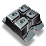
SOT-227B, miniBLOC
E153432
Symbol
Test Conditions
Maximum Ratings
VCES
TJ = 25C to 150C
600
V
VCGR
TJ = 25C to 150C, RGE = 1M
600
V
VGES
Continuous
±20
V
VGEM
Transient
±30
V
IC25
IC110
ILRMS
ICM
TC = 25C (Chip Capability)
TC = 110C
Terminal Current Limit
TC = 25C, 1ms
400
190
200
800
A
A
A
A
SSOA
VGE = 15V, TVJ = 125C, RG = 0.5
ICM = 400
A
(RBSOA)
Clamped Inductive Load
PC
TC = 25C
E
G
E
C
G = Gate, C = Collector, E = Emitter
either emitter terminal can be used as
Main or Kelvin Emitter
@ 0.8 • VCES
830
W
TJ
-55 ... +150
C
Features
TJM
Tstg
150
-55 ... +150
C
C
2500
3000
V~
V~
1.5/13
1.3/11.5
Nm/lb.in.
Nm/lb.in.
30
g
VISOL
Md
50/60Hz
IISOL 1mA
t = 1min
t = 1s
Mounting Torque
Terminal Connection Torque (M4)
Weight
Optimized for Low Conduction losses
Square RBSOA
High Current Capability
Isolation Voltage 3000 V~
International Standard Package
Advantages
High Power Density
Low Gate Drive Requirement
Applications
Symbol
Test Conditions
(TJ = 25C, Unless Otherwise Specified)
Characteristic Values
Min.
Typ.
Max.
BVCES
IC
= 1mA, VGE = 0V
600
VGE(th)
IC
= 250uA, VCE = VGE
3.0
ICES
VCE = VCES, VGE = 0V
V
5.5
VCE = 0V, VGE = ±20V
VCE(sat)
IC
IC
V
250 μA
TJ = 125C
IGES
2.5 mA
±400 nA
= 100A, VGE = 15V, Note 1
= 400A
© 2016 IXYS CORPORATION, All Rights Reserved
1.05
1.55
1.25
V
V
Power Inverters
UPS
Motor Drives
SMPS
PFC Circuits
Battery Chargers
Welding Machines
Lamp Ballasts
Inrush Current Protection Circuits
DS99577C(12/16)
�IXGN400N60A3
Symbol
Test Conditions
(TJ = 25C, Unless Otherwise Specified)
Characteristic Values
Min.
Typ.
Max.
gfs
85
IC = 60A, VCE = 10V, Note 1
140
Cies
Coes
32
VCE = 25V, VGE = 0 V, f = 1MHz
Qge
IC = 100V, VGE = 15V, VCE = 0.5 • VCES
Qgc
td(on)
tr
td(off)
tf
td(on)
tr
td(off)
tf
VCE = 400V, RG = 0.5
VCE = 400V, RG = 0.5
nF
c
S
P
NUT MATERIAL:
STANDARD - Low carbon steel with
Ni plating.
OPTIONAL - Brass Nut is available
PART NUMBER-BN
870
nC
nC
300
nC
25
ns
95
ns
170
ns
270
ns
27
ns
97
ns
190
ns
650
ns
A
VMWN
pF
120
B
D
T
pF
Resistive load, TJ = 125°C
IC = 100A, VGE = 15V
S
66
Resistive load, TJ = 25C
IC = 100A, VGE = 15V
M4-7 NUT
(4 PLACES)
J
K
1450
Cres
Qg(on)
TO-227 Outline
E
F
G
H
Q
O
R
U
0.15 C/W
RthJC
RthCK
0.05
C/W
Note 1. Pulse test, t 300μs; duty cycle, d 2%.
IXYS Reserves the Right to Change Limits, Test Conditions, and Dimensions.
IXYS MOSFETs and IGBTs are covered
4,835,592
by one or more of the following U.S. patents: 4,860,072
4,881,106
4,931,844
5,017,508
5,034,796
5,049,961
5,063,307
5,187,117
5,237,481
5,381,025
5,486,715
6,162,665
6,259,123 B1
6,306,728 B1
6,404,065 B1
6,534,343
6,583,505
6,683,344
6,727,585
7,005,734 B2
6,710,405 B2 6,759,692
7,063,975 B2
6,710,463
6,771,478 B2 7,071,537
7,157,338B2
�IXGN400N60A3
Fig. 1. Extended Output Characteristics @ TJ = 25ºC
Fig. 2. Output Characteristics @ TJ = 125ºC
200
350
VGE = 15V
11V
9V
180
300
VGE = 15V
9V
160
140
I C - Amperes
I C - Amperes
250
7V
200
150
7V
120
100
80
5V
60
100
40
5V
50
20
0
0
0
0.5
1
1.5
2
0
2.5
0.5
1
VCE - Volts
Fig. 3. Dependence of VCE(sat) on
Junction Temperature
1.06
TJ = 25ºC
2.4
0.98
2.2
I C = 200A
I C = 300A
200A
100A
2.0
0.94
VCE - Volts
VCE(sat) - Normalized
Fig. 4. Collector-to-Emitter Voltage
vs. Gate-to-Emitter Voltage
2.6
VGE = 15V
1.02
1.5
VCE - Volts
0.90
0.86
1.8
1.6
1.4
0.82
1.2
I C = 100A
0.78
1.0
0.74
0.8
-50
-25
0
25
50
75
100
125
150
4
5
6
7
8
9
10
11
12
13
14
15
180
200
VGE - Volts
TJ - Degrees Centigrade
Fig. 6. Transconductance
Fig. 5. Input Admittance
200
240
180
160
I C - Amperes
g f s - Siemens
200
140
TJ = 125ºC
25ºC
- 40ºC
120
100
80
TJ = - 40ºC
25ºC
125ºC
160
120
80
60
40
40
20
0
0
3.5
4.0
4.5
5.0
5.5
VGE - Volts
© 2016 IXYS CORPORATION, All Rights Reserved
6.0
6.5
0
20
40
60
80
100
I C - Amperes
120
140
160
�IXGN400N60A3
Fig. 8. Reverse-Bias Safe Operating Area
Fig. 7. Gate Charge
450
16
400
VCE = 300V
14
I C = 100A
I C - Amperes
V GE - Volts
350
I G = 10mA
12
10
8
6
300
250
200
150
4
TJ = 125ºC
100
2
RG = 0.5Ω
dv / dt < 10V / ns
50
0
0
0
100
200
300
400
500
600
700
800
900
100
200
QG - NanoCoulombs
400
500
600
VCE - Volts
Fig. 10. Maximum Transient Thermal Impedance
Fig. 9. Capacitance
1
100,000
Cies
10,000
1,000
Z (th)JC - K / W
Capacitance - PicoFarads
300
Coes
0.1
0.01
100
Cres
f = 1 MHz
10
0
5
10
15
20
25
30
35
40
VCE - Volts
IXYS Reserves the Right to Change Limits, Test Conditions, and Dimensions.
0.001
0.0001
0.001
0.01
0.1
Pulse Width - Seconds
1
10
�IXGN400N60A3
Fig. 12. Resistive Turn-on Rise Time
vs. Collector Current
Fig. 11. Resistive Turn-on Rise Time
vs. Junction Temperature
600
500
RG = 0.5Ω , VGE = 15V
450
I C = 300A
500
VCE = 400V
t r - Nanoseconds
t r - Nanoseconds
400
RG = 0.5ΩVGE = 15V
400
VCE = 400V
I C = 200A
300
200
TJ = 125ºC
350
300
TJ = 25ºC
250
200
150
100
100
I C = 100A
50
0
25
35
45
55
65
75
85
95
105
115
100
125
120
140
160
180
tr
600
50
I C = 300A, 200A, 100A
40
100
30
0
2.5
3.0
3.5
4.0
4.5
td(off)
550
500
190
450
180
400
170
I C = 300A
350
150
250
140
25
35
45
65
75
85
95
105
115
130
125
Fig. 16. Resistive Turn-off Switching Times
vs. Gate Resistance
500
190
TJ = 125ºC
400
180
170
TJ = 25ºC
160
td(off)
RG = 0.5Ω, VGE = 15V
150
t f - Nanoseconds
200
700
380
650
340
tf
600
td(off)
I C = 100A
300
TJ = 125ºC, VGE =15V
VCE = 400V
I C = 200A
550
260
I C = 300A
500
220
450
t d(off) - Nanoseconds
600
t d(off) - Nanoseconds
t f - Nanoseconds
55
TJ - Degrees Centigrade
210
tf
160
300
5.0
700
100
200
I C = 100A, 200A
Fig. 15. Resistive Turn-off Switching Times
vs. Collector Current
200
210
VCE = 400V
RG - Ohms
300
220
200
20
2.0
t f - Nanoseconds
t r - Nanoseconds
60
300
1.5
300
t d(off) - Nanoseconds
I C = 300A
t d(on) - Nanoseconds
70
1.0
280
RG = 0.5Ω, VGE = 15V
600
VCE = 400V
500
0.5
260
230
tf
650
80
TJ = 125ºC, VGE = 15V
200
240
700
90
td(on)
400
220
Fig. 14. Resistive Turn-off Switching Times
vs. Junction Temperature
Fig. 13. Resistive Turn-on Switching Times
vs. Gate Resistance
700
200
I C - Amperes
TJ - Degrees Centigrade
180
VCE = 400V
0
100
120
140
160
180
200
220
240
I C - Amperes
© 2016 IXYS CORPORATION, All Rights Reserved
260
280
140
300
400
140
0.5
1.0
1.5
2.0
2.5
3.0
3.5
4.0
4.5
5.0
RG - Ohms
IXYS REF: G_400N60A3(99)7-10-08-C
�Disclaimer Notice - Information furnished is believed to be accurate and reliable. However, users should independently
evaluate the suitability of and test each product selected for their own applications. Littelfuse products are not designed for,
and may not be used in, all applications. Read complete Disclaimer Notice at www.littelfuse.com/disclaimer-electronics.
�


 工商网监
湘ICP备2023018690号
工商网监
湘ICP备2023018690号
