FGD3N60LSD IGBT
FGD3N60LSD
IGBT
Description
Features
• High Current Capability
• Very Low Saturation Voltage : VCE(sat) = 1.2 V @ IC = 3A
ON Semiconductor's Insulated Gate Bipolar Transistors
(IGBTs)
provide very low conduction losses. The device is
designed for applica-tions where very low On-Voltage Drop is
a required feature.
• High Input Impedance
Applications
• HID Lamp Applications
• Piezo Fuel Injection Applications
C
C
G
G
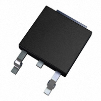
D-PAK
E
E
Absolute Maximum Ratings
Symbol
Description
FGD3N60LSD
Units
VCES
Collector-Emitter Voltage
600
V
VGES
Gate-Emitter Voltage
± 25
V
IC
Collector Current
@ TC = 25°C
6
A
Collector Current
@ TC = 100°C
3
A
25
A
3
A
ICM (1)
Pulsed Collector Current
IF
Diode Continous Forward Current
(1)
@ TC = 100°C
I FM
Diode Maximum Forward Current
PD
Maximum Power Dissipation
TJ
Operating Junction Temperature
Tstg
Storage Temperature Range
-55 to +150
°C
TL
Maximum Lead Temp. for Soldering
Purposes, 1/8” from Case for 5 Seconds
250
°C
25
A
40
W
0.32
W/°C
-55 to +150
°C
@ TC = 25°C
Derating Factor
Notes :
(1) Repetitive rating : Pulse width limited by max. junction temperature
Thermal Characteristics
Symbol
RθJC (IGBT)
RθJA
Typ.
Max.
Units
Thermal Resistance, Junction-to-Case
Parameter
--
3.1
°C/W
Thermal Resistance, Junction-to-Ambient (PCB Mount) (2)
--
100
°C/W
Notes :
(2) Mounted on 1” squre PCB (FR4 or G-10 Material)
©2006 Semiconductor Components Industries, LLC.
October-2017,Rev. 2
Publication Order Number:
FGD3N60LSD/D
�Device Marking
Device
Package
Reel Size
Tape Width
Quantity
FGD3N60LSD
FGD3N60LSDTM
D-PAK
380mm
16mm
2500
Electrical Characteristics of the IGBT
Symbol
Parameter
TC = 25°C unless otherwise noted
Test Conditions
Min.
Typ.
Max.
Units
Off Characteristics
BVCES
Collector-Emitter Breakdown Voltage
VGE = 0V, IC = 250uA
600
--
--
V
∆BVCES/
∆TJ
Temperature Coefficient of Breakdown
Voltage
VGE = 0V, IC = 1mA
--
0.6
--
V/°C
ICES
Collector Cut-Off Current
VCE = VCES, VGE = 0V
--
--
250
uA
IGES
G-E Leakage Current
VGE = VGES, VCE = 0V
--
--
± 100
nA
IC = 3mA, VCE = VGE
2.5
3.2
5.0
V
On Characteristics
VGE(th)
G-E Threshold Voltage
VCE(sat)
Collector to Emitter
Saturation Voltage
IC = 3A,
VGE = 10V
--
1.2
1.5
V
IC = 6A,
VGE = 10V
--
1.8
--
V
Dynamic Characteristics
Cies
Input Capacitance
Coes
Output Capacitance
Cres
Reverse Transfer Capacitance
VCE = 25V, VGE = 0V,
f = 1MHz
--
185
--
pF
--
20
--
pF
--
5.5
--
pF
--
40
--
ns
Switching Characteristics
td(on)
Turn-On Delay Time
tr
Rise Time
td(off)
Turn-Off Delay Time
tf
Eon
VCC = 480 V, IC = 3A,
RG = 470Ω, VGE = 10V,
Inductive Load, TC = 25°C
--
40
--
ns
--
600
--
ns
Fall Time
--
600
--
ns
Turn-On Switching Loss
--
250
--
uJ
Eoff
Turn-Off Switching Loss
--
1.00
--
mJ
Ets
Total Switching Loss
--
1.25
--
mJ
--
40
--
ns
--
45
--
ns
td(on)
Turn-On Delay Time
tr
Rise Time
VCC = 480 V, IC = 3A,
RG = 470Ω, VGE = 10V,
Inductive Load, TC = 125°C
td(off)
Turn-Off Delay Time
--
620
--
ns
tf
Fall Time
--
800
--
ns
Eon
Turn-On Switching Loss
--
300
--
uJ
Eoff
Turn-Off Switching Loss
--
1.9
--
mJ
--
2.2
--
mJ
--
12.5
--
nC
--
2.8
--
nC
--
4.9
--
nC
--
7.5
--
nH
Ets
Total Switching Loss
Qg
Total Gate Charge
Qge
Gate-Emitter Charge
Qgc
Gate-Collector Charge
Le
Internal Emitter Inductance
VCE = 480 V, IC = 3A,
VGE = 10V
Measured 5mm from PKG
www.onsemi.com
2
FGD3N60LSD IGBT
Package Marking and Ordering Information
�C
Symbol
VFM
trr
Irr
Qrr
= 25°C unless otherwise noted
Parameter
Diode Forward Voltage
Diode Reverse Recovery Time
Diode Peak Reverse Recovery Current
Test Conditions
IF = 3A
IF = 3A,
di/dt = 100A/us
VR = 200V
Diode Reverse Recovery Charge
www.onsemi.com
3
Min.
Typ.
Max.
Units
V
TC = 25°C
--
1.5
1.9
TC = 100°C
--
1.55
--
TC = 25°C
--
234
--
TC = 100°C
--
--
--
TC = 25°C
--
2.64
--
TC = 100°C
--
--
--
TC = 25°C
--
309
--
TC = 100°C
--
--
--
ns
A
nC
FGD3N60LSD IGBT
Electrical Characteristics of DIODE T
�FGD3N60LSD IGBT
Typical Performance Characteristics
Figure 1. Typical Output Characteristics
30
Figure 2. Typical Output Characteristics
30
Common Emitter
T C = 25 ° C
20V
Common Emitter
TC = 125°C
15V
Collector Current, IC [A]
Collector Current, IC [A]
24
10V
18
V GE = 8V
12
6
20V
24
15V
18
10V
VGE = 8V
12
6
0
0
2
4
6
8
0
0
Collector-Emitter Voltage, V CE [V]
Figure 3. Typical Output Characteristics
10
T C = 25 ° C
Collector Current, IC [A]
Collector Current, IC [A]
Common Emitter
V GE = 10V
T C = 125 ° C
6
4
2
8
Common Emitter
V CE = 20V
T C = 25 °C
T C = 125° C
6
4
2
0
0
0.1
1
10
1
Figure 5. Saturation Voltage vs. Case
3
Figure 6. Capacitance Characteristics
600
Comm on Emitter
V GE = 10V
Com m on Em itter
V GE = 0V, f = 1MHz
T C = 25 ° C
Capacitance [pF]
500
2
IC = 6A
IC = 3A
1
10
Gate-Emitter Voltage, V GE[V]
Collector-Emitter Voltage, V CE[V]
Collector-Emitter Voltage, VCE [V]
8
Figure 4. Transfer Characteristics
10
8
2
4
6
Collector-Emitter Voltage, VCE [V]
IC = 1.5A
400
Cies
300
Coes
200
Cres
100
0
0
0
30
60
90
120
150
1
Case Temperature, T C [° C]
10
Collector - Emitter Voltage, V CE [V]
www.onsemi.com
4
�Figure 7. Gate Charge
12
Figure 8. Turn-On Characteristics vs. Gate
Resistance
1000
C o m m o n E m itte r
V CC = 4 8 0 V , V GE = 1 0 V
Vcc = 480V
T C = 25 ° C
IC = 3 A
Switching Time [ns]
Gate - Emitter Voltage, VGE [V]
(Continued)
Com m on Em itter
R L = 160 Ω
10
FGD3N60LSD IGBT
Typical Performance Characteristics
8
6
4
T C = 25°C
T C = 125°C
T on
100
Tr
2
0
0
2
4
6
8
10
10
12
200
400
600
800 1000
G ate R esistance, R G [ Ω ]
Gate Charge, Q g [nC]
Figure 9. Turn-Off Characteristics vs.
Gate Resistance
Figure 10. Switching Loss vs. Gate Resistance
10000
10000
Com m on Em itter
V CC = 480V, V GE = 10V
IC = 3A
Eoff
T C = 125 ° C
Switching Loss [µJ]
Switching Time [ns]
T C = 25 ° C
Toff
1000
Tf
1000
Eon
100
Com m on Em itter
V CC = 480V, V GE = 10V
IC = 3A
T C = 25 ° C
100
200
400
600
T C = 125 °C
10
800 1000
200
400
Gate Resistance, R G [ Ω ]
Gate Resistance, R G [Ω ]
Figure 11. Turn-On Characteristics vs.
Collector Current
600
800 1000
Figure 12. Turn-Off Characteristics vs.
Collector Current
Common Emitter
Vcc = 480V, V GE = 10V
RG = 470 Ω
100
1000
T C = 125 ° C
Toff
Switching Time [ns]
Switching Time [ns]
T C = 25° C
Ton
Tr
Tf
Common Emitter
Vcc = 480 V, VGE = 10V
RG = 470Ω
T C = 25 ° C
T C = 125° C
10
2
3
Collector Current, IC [A]
100
4
2
www.onsemi.com
5
3
Collector Current, IC [A]
4
�FGD3N60LSD IGBT
Typical Performance Characteristics
(Continued)
Figure 13. Switching Loss vs. Collector Current
Figure 14. Forward Characteristics
100
Tc = 25°C
Tc = 100°C
Common Emitter
Vcc = 480 V, VGE = 10V
RG = 470Ω
TC = 25°C
Forward Current, IF [A]
Switching Loss [µJ]
TC = 125°C
Eoff
1000
Eon
10
1
100
0.1
2
3
Collector Current, IC [A]
0
4
Figure 15. Forward Voltage Drop Vs Tj
1
2
3
4
Forward Voltage Drop, VF [V]
Figure 16. SOA Characteristics
100
2.8
Collector Current, Ic [A]
2.4
IF=6 A
2.0
1.6
IF=3 A
50µs
10
100µs
Ic MAX (Continuous)
1ms
1
DC Operation
Single Nonrepetitive
Pulse Tc = 25°C
Curves must be derated
linearly with increase
in temperature
0.1
IF=1.5 A
1.2
0.01
25
50
75
100
125
0.1
Junction Temperature, Tj [°C]
1
10
100
Collector - Emitter Voltage, VCE [V]
Figure 17. Transient Thermal Impedance of IGBT
10
0 .5
Thermal Response [Zthjc]
Forward Voltage Drop, VF [V]
Ic MAX (Pulsed)
1
0 .2
0 .1
0 .0 5
0 .1
0 .0 2
Pdm
s in g le p u ls e
t1
0 .0 1
t2
0 .0 1
1 E -5
Duty factor D = t1 / t2
Peak Tj = Pdm × Zthjc + TC
1 E -4
1 E -3
0 .0 1
0 .1
R e c ta ngula r P uls e D ura tio n [s e c ]
www.onsemi.com
6
1
10
1000
�FGD3N60LSD IGBT
Mechanical Dimensions
D-PAK
Dimensions in Millimeters
www.onsemi.com
7
�ON Semiconductor and
are trademarks of Semiconductor Components Industries, LLC dba ON Semiconductor or its subsidiaries in the United States and/or other countries.
ON Semiconductor owns the rights to a number of patents, trademarks, copyrights, trade secrets, and other intellectual property. A listing of ON Semiconductor’s product/patent
coverage may be accessed at www.onsemi.com/site/pdf/Patent−Marking.pdf. ON Semiconductor reserves the right to make changes without further notice to any products herein.
ON Semiconductor makes no warranty, representation or guarantee regarding the suitability of its products for any particular purpose, nor does ON Semiconductor assume any liability
arising out of the application or use of any product or circuit, and specifically disclaims any and all liability, including without limitation special, consequential or incidental damages.
Buyer is responsible for its products and applications using ON Semiconductor products, including compliance with all laws, regulations and safety requirements or standards,
regardless of any support or applications information provided by ON Semiconductor. “Typical” parameters which may be provided in ON Semiconductor data sheets and/or
specifications can and do vary in different applications and actual performance may vary over time. All operating parameters, including “Typicals” must be validated for each customer
application by customer’s technical experts. ON Semiconductor does not convey any license under its patent rights nor the rights of others. ON Semiconductor products are not
designed, intended, or authorized for use as a critical component in life support systems or any FDA Class 3 medical devices or medical devices with a same or similar classification
in a foreign jurisdiction or any devices intended for implantation in the human body. Should Buyer purchase or use ON Semiconductor products for any such unintended or unauthorized
application, Buyer shall indemnify and hold ON Semiconductor and its officers, employees, subsidiaries, affiliates, and distributors harmless against all claims, costs, damages, and
expenses, and reasonable attorney fees arising out of, directly or indirectly, any claim of personal injury or death associated with such unintended or unauthorized use, even if such
claim alleges that ON Semiconductor was negligent regarding the design or manufacture of the part. ON Semiconductor is an Equal Opportunity/Affirmative Action Employer. This
literature is subject to all applicable copyright laws and is not for resale in any manner.
PUBLICATION ORDERING INFORMATION
LITERATURE FULFILLMENT:
Literature Distribution Center for ON Semiconductor
19521 E. 32nd Pkwy, Aurora, Colorado 80011 USA
Phone: 303−675−2175 or 800−344−3860 Toll Free USA/Canada
Fax: 303−675−2176 or 800−344−3867 Toll Free USA/Canada
Email: orderlit@onsemi.com
❖
© Semiconductor Components Industries, LLC
N. American Technical Support: 800−282−9855 Toll Free
USA/Canada
Europe, Middle East and Africa Technical Support:
Phone: 421 33 790 2910
Japan Customer Focus Center
Phone: 81−3−5817−1050
ON Semiconductor Website: www.onsemi.com
Order Literature: http://www.onsemi.com/orderlit
For additional information, please contact your local
Sales Representative
www.onsemi.com
�


 工商网监
湘ICP备2023018690号
工商网监
湘ICP备2023018690号
