Si52144
PCI-E XPRESS G EN 1, G EN 2 , & G EN 3 C LOCK Q UAD O UTPUT G ENERAT OR
Features
PCI-Express Gen 1, Gen 2, & Gen 3 Compliant Low power push-pull type differential output buffers Integrated resistors on differential clocks Dedicated output enable hardware pin for each clock Hardware selectable spread control Four PCI-Express Clocks
25 MHz crystal input or clock input
I2C support with readback capabilities Triangular spread spectrum profile for maximum electromagnetic interference (EMI) reduction Industrial temperature: –40 to 85 oC 3.3 V power supply 24-pin QFN package
Ordering Information: See page 18
Applications
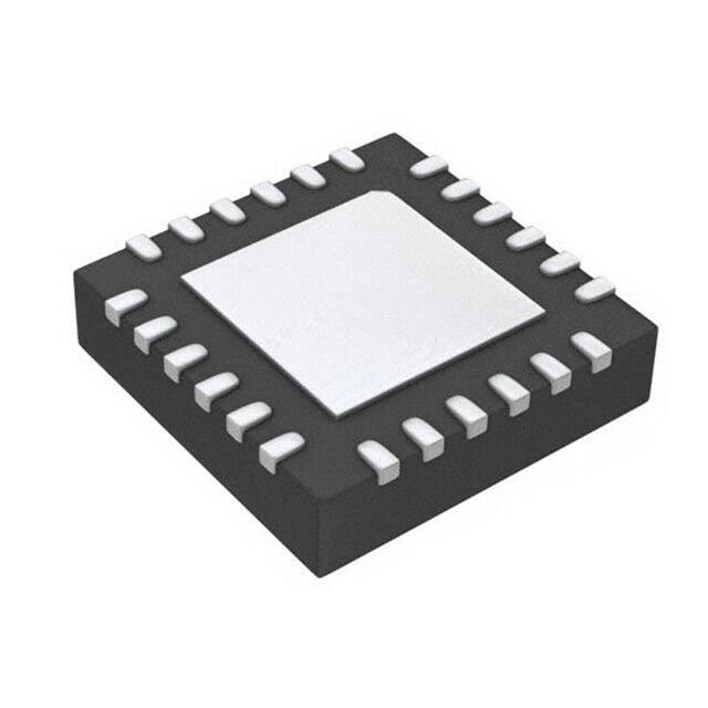
Pin Assignments
VDD_CORE VSS_CORE XIN/CLKIN
SDATA
20
24
23
22
XOUT
21
Description
The Si52144 is a spread-controlled PCIe clock generator that can source four PCIe clocks simultaneously. The device has four hardware output enable control inputs for enabling the respective differential outputs on the fly while powered on along with the spread control hardware pin to enable spread for EMI reduction. In addition to the hardware control pins, I2C programmability is also available to promptly achieve optimum clock signal integrity through skew and edge rate control on true, compliment, or both differential outputs as well as amplitude control.
SCLK
19
1 18 OE3
Network attached storage Multi-function printer
Wireless access point Routers
VDD OE1
1
1 2 3 4 5 6 7 8 9 10 11 12
17 VDD 16 DIFF3 15 DIFF3 14 DIFF2 13 DIFF2
SSON2 VSS OE21 VDD
25 GND
DIFF0
DIFF1
DIFF1
Notes: 1. Internal 100 kohm pull-up. 2. Internal 100 kohm pull-down.
Functional Block Diagram
Patents pending
XIN/CLKIN XOUT
DIFF0
DIFF1
PLL (SSC)
Divider
DIFF2
DIFF3 SCLK SDATA OE [3:0] SSON
Control & Memory
Control RAM
Preliminary Rev. 0.1 12/11
Copyright © 2011 by Silicon Laboratories
DIFF0
OE01
VDD
Si52144
This information applies to a product under development. Its characteristics and specifications are subject to change without notice.
�S i52144
2
Preliminary Rev. 0.1
�S i52144 TABLE O F C ONTENTS
Section Page
1. Electrical Specifications . . . . . . . . . . . . . . . . . . . . . . . . . . . . . . . . . . . . . . . . . . . . . . . . . . .4 2. Functional Description . . . . . . . . . . . . . . . . . . . . . . . . . . . . . . . . . . . . . . . . . . . . . . . . . . . .7 2.1. Crystal Recommendations . . . . . . . . . . . . . . . . . . . . . . . . . . . . . . . . . . . . . . . . . . . . .7 2.2. OE Clarification . . . . . . . . . . . . . . . . . . . . . . . . . . . . . . . . . . . . . . . . . . . . . . . . . . . . . .8 2.3. OE Assertion . . . . . . . . . . . . . . . . . . . . . . . . . . . . . . . . . . . . . . . . . . . . . . . . . . . . . . . .8 2.4. OE Deassertion . . . . . . . . . . . . . . . . . . . . . . . . . . . . . . . . . . . . . . . . . . . . . . . . . . . . . .8 2.5. SSON Clarification . . . . . . . . . . . . . . . . . . . . . . . . . . . . . . . . . . . . . . . . . . . . . . . . . . .8 3. Test and Measurement Setup . . . . . . . . . . . . . . . . . . . . . . . . . . . . . . . . . . . . . . . . . . . . . . .9 4. Control Registers . . . . . . . . . . . . . . . . . . . . . . . . . . . . . . . . . . . . . . . . . . . . . . . . . . . . . . . .11 4.1. Serial Data Interface . . . . . . . . . . . . . . . . . . . . . . . . . . . . . . . . . . . . . . . . . . . . . . . . .11 4.2. Data Protocol . . . . . . . . . . . . . . . . . . . . . . . . . . . . . . . . . . . . . . . . . . . . . . . . . . . . . .11 5. Pin Descriptions: 24-Pin QFN . . . . . . . . . . . . . . . . . . . . . . . . . . . . . . . . . . . . . . . . . . . . . . 16 6. Ordering Guide . . . . . . . . . . . . . . . . . . . . . . . . . . . . . . . . . . . . . . . . . . . . . . . . . . . . . . . . . . 18 7. Package Outline . . . . . . . . . . . . . . . . . . . . . . . . . . . . . . . . . . . . . . . . . . . . . . . . . . . . . . . . . 19 Contact Information . . . . . . . . . . . . . . . . . . . . . . . . . . . . . . . . . . . . . . . . . . . . . . . . . . . . . . . .20
Preliminary Rev. 0.1
3
�S i52144
1. Electrical Specifications
Table 1. DC Electrical Specifications
Parameter 3.3 V Operating Voltage 3.3 V Input High Voltage 3.3 V Input Low Voltage Input High Voltage Input Low Voltage Input High Leakage Current Input Low Leakage Current 3.3 V Output High Voltage (SE) 3.3 V Output Low Voltage (SE) High-impedance Output Current Input Pin Capacitance Output Pin Capacitance Pin Inductance Dynamic Supply Current Symbol VDD core VIH VIL VIHI2C VILI2C IIH IIL VOH VOL IOZ CIN COUT LIN IDD_3.3V All outputs enabled. Differential clocks with 5” traces and 2 pF load. Test Condition 3.3 ±5% Control input pins Control input pins SDATA, SCLK SDATA, SCLK Except internal pull-down resistors, 0 < VIN < VDD Except internal pull-up resistors, 0 < VIN < VDD IOH = –1 mA IOL = 1 mA Min 3.135 2.0 VSS – 0.3 2.2 — — –5 2.4 — –10 1.5 — — — Typ 3.3 — — — — — — — — — — — — — Max 3.465 VDD + 0.3 0.8 — 1.0 5 — — 0.4 10 5 6 7 50 Unit V V V V V A A V V A pF pF nH mA
4
Preliminary Rev. 0.1
�S i52144
Table 2. AC Electrical Specifications
Parameter Crystal Long-term Accuracy Clock Input CLKIN Duty Cycle CLKIN Rise and Fall Times CLKIN Cycle to Cycle Jitter CLKIN Long Term Jitter Input High Voltage Input Low Voltage Input High Current Input Low Current DIFF at 0.7 V
DIFF Duty Cycle
Symbol LACC TDC TR/TF TCCJ TLTJ VIH VIL IIH IIL TDC
Condition Measured at VDD/2 differential Measured at VDD/2 Measured between 0.2 VDD and 0.8 VDD Measured at VDD/2 Measured at VDD/2 XIN/CLKIN pin XIN/CLKIN pin XIN/CLKIN pin, VIN = VDD XIN/CLKIN pin, 0 < VIN
很抱歉,暂时无法提供与“SI52144-A01AGMR”相匹配的价格&库存,您可以联系我们找货
免费人工找货- 国内价格
- 1+29.85120
- 10+29.14920
- 30+28.68480