STD60N3LH5
N-channel 30 V, 0.0072 Ω typ., 48 A STripFET™ V Power MOSFET
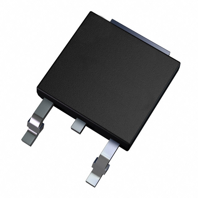
in a DPAK package
Datasheet - not recommended for new design
Features
Order code
VDS @ Tjmax RDS(on) max
STD60N3LH5
TAB
ID
0.008 Ω
35 V
48 A
)
s
(
ct
• RDS(on) * Qg industry benchmark
3
• Extremely low on-resistance RDS(on)
u
d
o
1
• Very low switching gate charge
DPAK
r
P
e
• High avalanche ruggedness
• Low gate drive power losses
t
e
l
o
Applications
Figure 1. Internal schematic diagram
)
(s
'����7$%�
t
c
u
d
o
r
*���
P
e
let
o
s
b
s
b
ODescription
• Switching applications
This device is an N-channel Power MOSFET
developed using STMicroelectronics’
STripFET™V technology. The device has been
optimized to achieve very low on-state resistance,
contributing to a FOM that is among the best in its
class.
6���
$0�����Y�
O
Table 1. Device summary
Order code
Marking
Packages
Packaging
STD60N3LH5
60N3LH5
DPAK
Tape and reel
August 2013
DocID14079 Rev 5
This is information on a product in full production. This is information on a product still in production but not recommended
for new designs.
1/19
www.st.com
�Contents
STD60N3LH5
Contents
1
Electrical ratings . . . . . . . . . . . . . . . . . . . . . . . . . . . . . . . . . . . . . . . . . . . . 3
2
Electrical characteristics . . . . . . . . . . . . . . . . . . . . . . . . . . . . . . . . . . . . . 4
2.1
Electrical characteristics (curves)
............................ 6
3
Test circuits
.............................................. 8
4
Package mechanical data . . . . . . . . . . . . . . . . . . . . . . . . . . . . . . . . . . . . 10
5
Revision history . . . . . . . . . . . . . . . . . . . . . . . . . . . . . . . . . . . . . . . . . . . 14
)
s
(
ct
u
d
o
r
P
e
t
e
l
o
)
(s
s
b
O
t
c
u
d
o
r
P
e
t
e
l
o
s
b
O
2/19
DocID14079 Rev 5
�STD60N3LH5
1
Electrical ratings
Electrical ratings
Table 2. Absolute maximum ratings
Symbol
Parameter
Value
Unit
VDS
Drain-source voltage
30
V
VDS
Drain-source voltage @ Tjmax
35
V
VGS
Gate-source voltage
± 20
V
ID (1)
Drain current (continuous) at TC = 25 °C
48
A
ID
Drain current (continuous) at TC = 100 °C
42.8
Drain current (pulsed)
192
Total dissipation at TC = 25 °C
60
IDM
(2)
PTOT
EAS
0.4
P
e
Single pulse avalanche energy
Tj
Tstg
A
du
ro
Derating factor
(3)
)
s
(
ct
A
W
W/°C
160
mJ
-55 to 175
°C
Value
Unit
Thermal resistance junction-case max.
2.5
°C/W
Thermal resistance junction-pcb max.
50
°C/W
let
Operating junction temperature
Storage temperature
o
s
b
1. Limited by wire bonding.
2. Pulse width limited by safe operating area.
O
)
3. Starting Tj = 25 °C, ID = 24 A, VDD = 12 V.
s
(
t
c
Table 3. Thermal resistance
du
Symbol
ro
Rthj-case
P
e
Rthj-pcb(1)
Parameter
t
e
l
o
1. When mounted on FR-4 board of 1inch², 2oz Cu
s
b
O
DocID14079 Rev 5
3/19
19
�Electrical characteristics
2
STD60N3LH5
Electrical characteristics
(TCASE = 25 °C unless otherwise specified)
Table 4. Static
Symbol
Parameter
Test conditions
Drain-source breakdown
Voltage
ID = 250 µA, VGS= 0
IDSS
Zero gate voltage drain
current (VGS = 0)
VDS = 30 V
VDS = 30 V, TC = 125 °C
IGSS
Gate body leakage current
(VDS = 0)
VGS = ± 20 V
VGS(th)
Gate threshold voltage
VDS= VGS, ID = 250 µA
RDS(on)
Static drain-source
on-resistance
VGS= 10 V, ID= 24 A
V(BR)DSS
VGS= 5 V, ID= 24 A
e
t
e
ol
Min.
Typ.
Max.
30
Unit
V
1
10
µA
µA
±100
nA
)
s
(
ct
du
3
V
0.0072
0.008
Ω
0.0088
0.011
Ω
Min.
Typ.
Max.
Unit
-
1350
1620
pF
-
265
318
pF
-
32
38
pF
-
8.8
12.3
nC
-
4.7
6.6
nC
-
2.2
3.1
nC
-
2.2
3.1
nC
-
2.5
3.5
nC
-
1.1
1.3
Ω
1
1.8
o
r
P
Table 5. Dynamic
Symbol
Ciss
Input capacitance
Coss
Output capacitance
Crss
Reverse transfer
capacitance
Qg
Total gate charge
Qgs
e
t
e
ol
Qgd
bs
O
)-
s
(
t
c
u
d
o
VDS =25 V, f=1 MHz,
VGS=0
VDD=15 V, ID = 48 A
VGS =5 V
(Figure 14)
Pr
Gate-source charge
Gate-drain charge
Pre Vth gate-to-source
charge
Qgs2
Post Vth gate-to-source
charge
Gate input resistance
s
b
O
Test conditions
Qgs1
RG
4/19
Parameter
VDD=15 V, ID = 48 A
VGS =5 V
(Figure 19)
f = 1 MHz, gate DC
Bias = 0,
test signal level = 20 mV,
ID = 0
DocID14079 Rev 5
�STD60N3LH5
Electrical characteristics
Table 6. Switching on/off (resistive load)
Symbol
td(on)
tr
td(off)
tf
Parameter
Test conditions
Turn-on delay time
VDD=10 V, ID= 24 A,
RG=4.7 Ω, VGS= 10 V
(Figure 13 and
Figure 18)
Rise time
Turn-off delay time
Fall time
Min.
Typ.
Max.
Unit
-
6
-
ns
-
33
-
ns
-
19
-
ns
-
4.2
-
ns
Min.
Typ.
Max.
Table 7. Source drain diode
Symbol
ISD
Parameter
Test conditions
Source-drain current
uc
(1)
ISDM
Source-drain current (pulsed)
VSD
Forward on voltage
ISD=24 A, VGS=0
trr
Reverse recovery time
Qrr
Reverse recovery charge
IRRM
Reverse recovery current
od
-
ISD=48 A,
di/dt =100 A/µs,
VDD=20 V, (Figure 15)
1. Pulsed: pulse duration = 300µs, duty cycle 1.5%
o
s
b
e
t
e
l
Pr
)
s
(
t
-
Unit
48
A
192
A
1.1
V
-
25
ns
-
18.5
nC
-
1.5
A
O
)
s
(
t
c
u
d
o
r
P
e
t
e
l
o
s
b
O
DocID14079 Rev 5
5/19
19
�Electrical characteristics
2.1
STD60N3LH5
Electrical characteristics (curves)
Figure 2. Safe operating area
+9�����
,'
�$�
7M ���&
7F ��&
LV
D�
H
DU
���
Figure 3. Thermal impedance
6LQJOH
SXOVH
�
RQ
�
�
LV '6
�WK �5
LQ D[
Q�
LR \�P
W
UD �E
SH HG
2 LPLW
/
���V
�PV
��
��PV
�
���
���
�
��
���
)
s
(
ct
u
d
o
9'6�9�
Figure 4. Output characteristics
Figure 5. Transfer characteristics
r
P
e
ID
(A)
160
AM03360v1
t
e
l
o
140
s
b
O
120
100
)
(s
od
t
c
u
r
P
e
60
40
20
0
0
Figure 6. Normalized V(BR)DSS vs temperature
1
2
3
4
5
VGS(V)
Figure 7. Static drain-source on-resistance
t
e
l
o
s
b
O
6/19
80
DocID14079 Rev 5
�STD60N3LH5
Electrical characteristics
Figure 8. Gate charge vs gate-source voltage
Figure 10. Normalized gate threshold voltage vs
temperature
Figure 9. Capacitance variations
)
s
(
ct
u
d
o
Figure 11. Normalized on-resistance vs
temperature
r
P
e
t
e
l
o
)
(s
s
b
O
t
c
u
d
o
r
Figure 12. Source-drain diode forward
characteristics
P
e
t
e
l
o
s
b
O
DocID14079 Rev 5
7/19
19
�Test circuits
3
STD60N3LH5
Test circuits
Figure 13. Switching times test circuit for
resistive load
Figure 14. Gate charge test circuit
VDD
12V
47kΩ
1kΩ
100nF
3.3
μF
2200
RL
μF
IG=CONST
VDD
VGS
100Ω
Vi=20V=VGMAX
VD
RG
2200
μF
D.U.T.
VG
c
u
d
47kΩ
1kΩ
AM01468v1
e
t
e
ol
Figure 15. Test circuit for inductive load
switching and diode recovery times
A
A
G
D.U.T.
FAST
DIODE
B
B
S
s
(
t
c
3.3
μF
B
25 Ω
D
1000
μF
RG
S
r
P
e
s
b
O
2200
μF
3.3
μF
VDD
ID
Vi
D.U.T.
Pw
let
AM01470v1
AM01471v1
Figure 17. Unclamped inductive waveform
b
O
AM01469v1
L
VD
VDD
u
d
o
G
so
)-
L=100μH
o
r
P
Figure 16. Unclamped inductive load test circuit
A
D
)
s
(
t
2.7kΩ
PW
PW
D.U.T.
Figure 18. Switching time waveform
ton
V(BR)DSS
tdon
VD
toff
tr
tdoff
tf
90%
90%
IDM
10%
ID
VDD
10%
0
VDD
VDS
90%
VGS
AM01472v1
8/19
0
DocID14079 Rev 5
10%
AM01473v1
�STD60N3LH5
Test circuits
Figure 19. Gate charge waveform
)
s
(
ct
u
d
o
r
P
e
t
e
l
o
)
(s
s
b
O
t
c
u
d
o
r
P
e
t
e
l
o
s
b
O
DocID14079 Rev 5
9/19
19
�Package mechanical data
4
STD60N3LH5
Package mechanical data
In order to meet environmental requirements, ST offers these devices in different grades of
ECOPACK® packages, depending on their level of environmental compliance. ECOPACK®
specifications, grade definitions and product status are available at: www.st.com.
ECOPACK® is an ST trademark.
)
s
(
ct
u
d
o
r
P
e
t
e
l
o
)
(s
s
b
O
t
c
u
d
o
r
P
e
t
e
l
o
s
b
O
10/19
DocID14079 Rev 5
�STD60N3LH5
Package mechanical data
Table 8. DPAK (TO-252) type A mechanical data
mm
Dim.
Min.
Typ.
Max.
A
2.20
2.40
A1
0.90
1.10
A2
0.03
0.23
b
0.64
0.90
b4
5.20
5.40
c
0.45
0.60
c2
0.48
0.60
D
6.00
)
s
(
ct
6.20
D1
5.10
E
6.40
e
t
e
ol
E1
4.70
e
o
r
P
6.60
2.28
e1
4.40
H
9.35
L
1.00
(L1)
)-
s
b
O
s
(
t
c
L2
du
L4
ro
R
P
e
V2
du
4.60
10.10
1.50
2.80
0.80
0.60
1.00
0.20
0°
8°
t
e
l
o
s
b
O
DocID14079 Rev 5
11/19
19
�Package mechanical data
STD60N3LH5
Figure 20. DPAK (TO-252) type A drawing
)
s
(
ct
u
d
o
r
P
e
t
e
l
o
)
(s
s
b
O
t
c
u
d
o
r
P
e
t
e
l
o
s
b
O
0068772_K_type_A
12/19
DocID14079 Rev 5
�STD60N3LH5
Package mechanical data
Table 9. DPAK (TO-252) type E mechanical data
mm
Dim.
Min.
A
Typ.
Max.
2.18
2.39
A2
0.13
b
0.65
0.884
b4
4.95
5.46
c
0.46
0.61
c2
0.46
0.60
D
5.97
6.22
D1
5.21
E
6.35
E1
4.32
)
s
(
ct
u
d
o
e
2.286
t
e
l
o
e1
4.572
H
9.94
L
1.50
)-
L1
L2
0.89
s
b
O
s
(
t
c
L4
r
P
e
6.73
10.34
1.78
2.74
1.27
1.02
u
d
o
r
P
e
t
e
l
o
s
b
O
DocID14079 Rev 5
13/19
19
�Package mechanical data
STD60N3LH5
Figure 21. DPAK (TO-252) type E drawing
)
s
(
ct
u
d
o
r
P
e
t
e
l
o
)
(s
s
b
O
t
c
u
d
o
r
P
e
t
e
l
o
s
b
O
0068772_K_type_E
14/19
DocID14079 Rev 5
�STD60N3LH5
Package mechanical data
Figure 22. DPAK footprint (a)
)
s
(
ct
u
d
o
r
P
e
t
e
l
o
)
(s
s
b
O
t
c
u
Footprint_REV_K
d
o
r
P
e
t
e
l
o
s
b
O
a. All dimensions are in millimeters
DocID14079 Rev 5
15/19
19
�Packaging mechanical data
5
STD60N3LH5
Packaging mechanical data
Table 10. DPAK (TO-252) tape and reel mechanical data
Tape
Reel
mm
mm
Dim.
Dim.
Min.
Max.
A0
6.8
7
A
B0
10.4
10.6
B
1.5
12.1
C
12.8
1.6
D
20.2
G
16.4
B1
Min.
D
1.5
D1
1.5
E
1.65
1.85
N
F
7.4
7.6
T
K0
2.55
2.75
P0
3.9
4.1
P1
7.9
8.1
P2
1.9
2.1
R
40
T
0.25
W
15.7
t
c
u
)
(s
0.35
16.3
d
o
r
P
e
t
e
l
o
s
b
O
16/19
DocID14079 Rev 5
330
)
s
(
ct
13.2
u
d
o
r
P
e
50
t
e
l
o
s
b
O
Max.
18.4
22.4
Base qty.
2500
Bulk qty.
2500
�STD60N3LH5
Packaging mechanical data
Figure 23. Tape for DPAK (TO-252)
10 pitches cumulative
tolerance on tape +/- 0.2 mm
P0
Top cover
tape
T
P2
D
E
F
B1
W
K0
B0
For machine ref. only
including draft and
radii concentric around B0
A0
D1
P1
)
s
(
ct
User direction of feed
u
d
o
r
P
e
let
o
s
b
O
)
s
(
t
c
u
d
o
Bending radius
User direction of feed
AM08852v1
Figure 24. Reel for DPAK (TO-252)
T
r
P
e
REEL DIMENSIONS
40mm min.
t
e
l
o
s
b
O
R
Access hole
At slot location
B
D
C
N
A
Full radius
Tape slot
in core for
tape start 25 mm min.
width
G measured at hub
AM08851v2
DocID14079 Rev 5
17/19
19
�Revision history
6
STD60N3LH5
Revision history
Table 11. Document revision history
Date
Revision
Changes
19-Oct-2007
1
First release
23-Sep-2008
2
VGS value has been changed on Table 2 and Table 5
20-Apr-2009
3
– Inserted typical maximum value in VGS(th) parameter
– Figure 5: Transfer characteristics has been updated
– Added device in TO-220
05-Apr-2011
4
– Added device in Short IPAK
– Added max values in Table 5: Dynamic
– VGS value has been changed in Table 2 and Table 4
09-Aug-2013
5
The part numbers STP60N3LH5, STU60N3LH5 and STU60N3LH5-S
have been moved to a separate datasheet
u
d
o
r
P
e
t
e
l
o
)
(s
s
b
O
t
c
u
d
o
r
P
e
t
e
l
o
s
b
O
18/19
)
s
(
ct
DocID14079 Rev 5
�STD60N3LH5
)
s
(
ct
Please Read Carefully:
u
d
o
Information in this document is provided solely in connection with ST products. STMicroelectronics NV and its subsidiaries (“ST”) reserve the
right to make changes, corrections, modifications or improvements, to this document, and the products and services described herein at any
time, without notice.
All ST products are sold pursuant to ST’s terms and conditions of sale.
r
P
e
t
e
l
o
Purchasers are solely responsible for the choice, selection and use of the ST products and services described herein, and ST assumes no
liability whatsoever relating to the choice, selection or use of the ST products and services described herein.
s
b
O
No license, express or implied, by estoppel or otherwise, to any intellectual property rights is granted under this document. If any part of this
document refers to any third party products or services it shall not be deemed a license grant by ST for the use of such third party products
or services, or any intellectual property contained therein or considered as a warranty covering the use in any manner whatsoever of such
third party products or services or any intellectual property contained therein.
)
(s
UNLESS OTHERWISE SET FORTH IN ST’S TERMS AND CONDITIONS OF SALE ST DISCLAIMS ANY EXPRESS OR IMPLIED
WARRANTY WITH RESPECT TO THE USE AND/OR SALE OF ST PRODUCTS INCLUDING WITHOUT LIMITATION IMPLIED
WARRANTIES OF MERCHANTABILITY, FITNESS FOR A PARTICULAR PURPOSE (AND THEIR EQUIVALENTS UNDER THE LAWS
OF ANY JURISDICTION), OR INFRINGEMENT OF ANY PATENT, COPYRIGHT OR OTHER INTELLECTUAL PROPERTY RIGHT.
t
c
u
d
o
r
ST PRODUCTS ARE NOT AUTHORIZED FOR USE IN WEAPONS. NOR ARE ST PRODUCTS DESIGNED OR AUTHORIZED FOR USE
IN: (A) SAFETY CRITICAL APPLICATIONS SUCH AS LIFE SUPPORTING, ACTIVE IMPLANTED DEVICES OR SYSTEMS WITH
PRODUCT FUNCTIONAL SAFETY REQUIREMENTS; (B) AERONAUTIC APPLICATIONS; (C) AUTOMOTIVE APPLICATIONS OR
ENVIRONMENTS, AND/OR (D) AEROSPACE APPLICATIONS OR ENVIRONMENTS. WHERE ST PRODUCTS ARE NOT DESIGNED
FOR SUCH USE, THE PURCHASER SHALL USE PRODUCTS AT PURCHASER’S SOLE RISK, EVEN IF ST HAS BEEN INFORMED IN
WRITING OF SUCH USAGE, UNLESS A PRODUCT IS EXPRESSLY DESIGNATED BY ST AS BEING INTENDED FOR “AUTOMOTIVE,
AUTOMOTIVE SAFETY OR MEDICAL” INDUSTRY DOMAINS ACCORDING TO ST PRODUCT DESIGN SPECIFICATIONS.
PRODUCTS FORMALLY ESCC, QML OR JAN QUALIFIED ARE DEEMED SUITABLE FOR USE IN AEROSPACE BY THE
CORRESPONDING GOVERNMENTAL AGENCY.
P
e
t
e
l
o
s
b
O
Resale of ST products with provisions different from the statements and/or technical features set forth in this document shall immediately void
any warranty granted by ST for the ST product or service described herein and shall not create or extend in any manner whatsoever, any
liability of ST.
ST and the ST logo are trademarks or registered trademarks of ST in various countries.
Information in this document supersedes and replaces all information previously supplied.
The ST logo is a registered trademark of STMicroelectronics. All other names are the property of their respective owners.
© 2013 STMicroelectronics - All rights reserved
STMicroelectronics group of companies
Australia - Belgium - Brazil - Canada - China - Czech Republic - Finland - France - Germany - Hong Kong - India - Israel - Italy - Japan Malaysia - Malta - Morocco - Philippines - Singapore - Spain - Sweden - Switzerland - United Kingdom - United States of America
www.st.com
DocID14079 Rev 5
19/19
19
�