STGW30NC60VD
Datasheet
40 A, 600 V, fast IGBT with UltraFAST diode
Features
•
•
•
High current capability
High frequency operation up to 50 kHz
Very soft ultra fast recovery antiparallel diode
Applications
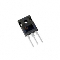
TO-247 long leads
•
•
•
High frequency inverters, UPS
Motor drive
SMPS and PFC in both hard switch and resonant topologies
Description
This device uses the advanced PowerMESH process resulting in an excellent tradeoff between switching performance and low on-state behavior.
SC12850_DIODE_IGBT
Product status link
STGW30NC60VD
Product summary
Order code
STGW30NC60VD
Marking
GW30NC60VD
Package
TO-247 long leads
Packing
Tube
DS5126 - Rev 6 - May 2022
For further information contact your local STMicroelectronics sales office.
www.st.com
�STGW30NC60VD
Electrical ratings
1
Electrical ratings
Table 1. Absolute maximum ratings
Symbol
Value
Unit
Collector-emitter voltage (VGE = 0 V)
600
V
Continuous collector current at TC = 25 °C
80
Continuous collector current at TC = 100 °C
40
ICL(2)
Turn-off latching current
100
A
ICP(3)
Pulsed collector current
150
A
VGE
Gate-emitter voltage
±20
V
Diode RMS forward current at TC = 25 °C
30
A
IFSM
Surge not repetitive forward current, tP = 10 ms sinusoidal
120
A
PTOT
Total power dissipation at TC = 25 °C
250
W
TJ
Operating junction temperature range
VCES
IC(1)
IF
TSTG
1.
Parameter
-55 to 150
Storage temperature range
Calculated according to the iterative formula: IC TC =
A
°C
°C
T J max − TC
Rtℎj − C × VCE sat max T J max , IC TC
2. Vclamp = 80% VCES, TJ =150 °C, RG = 10 Ω, VGE = 15 V.
3. Pulse width limited by maximum junction temperature and turn-off within RBSOA.
Table 2. Thermal data
Symbol
RthJC
RthJA
DS5126 - Rev 6
Parameter
Value
Unit
Thermal resistance, junction-to-case IGBT
0.5
°C/W
Thermal resistance, junction-to-case diode
1.5
°C/W
Thermal resistance, junction-to-ambient
50
°C/W
page 2/14
�STGW30NC60VD
Electrical characteristics
2
Electrical characteristics
TJ = 25 °C unless otherwise specified
Table 3. Static
Symbol
V(BR)CES
VCE(sat)
Parameter
Collector-emitter breakdown
voltage
Collector-emitter saturation
voltage
Test conditions
VGE = 0 V, IC = 1 mA
Typ.
VGE = 15 V, IC = 40 A
2.1
VGE = 15 V, IC = 80 A, TJ= 100 °C
2.9
VGE = 15 V, IC = 20 A, TJ= 125 °C
1.7
VCE = VGE, IC = 250 μA
ICES
Collector cut-off current
IGES
Gate-emitter leakage current
VCE = 0 V, VGE = ±20 V
Forward transconductance
VCE = 15 V, IC = 20 A
Unit
V
1.8
Gate threshold voltage
Max.
600
VGE = 15 V, IC = 20 A
VGE(th)
gfs
Min.
3.75
2.5
V
5.75
V
VGE = 0 V, VCE = 600 V
10
µA
VGE = 0 V, VCE = 600 V, TJ = 125 °C (1)
1
mA
±100
nA
15
S
1. Specified by design, not tested in production.
Table 4. Dynamic
Symbol
DS5126 - Rev 6
Parameter
Cies
Input capacitance
Coes
Output capacitance
Cres
Reverse transfer capacitance
Qg
Total gate charge
Qge
Gate-emitter charge
Qgc
Gate-collector charge
Test conditions
VCE = 25 V, f = 1 MHz, VGE = 0 V
VCE = 390 V, IC = 20 A, VGE = 15 V
(see Figure 17. Gate charge test circuit)
Min.
Typ.
-
2200
-
225
-
50
-
100
-
16
-
45
Max.
Unit
pF
140
nC
page 3/14
�STGW30NC60VD
Electrical characteristics
Table 5. Switching on/off (inductive load)
Symbol
td(on)
Parameter
Test conditions
Min.
Typ.
Max.
Unit
Turn-on delay time
VCC = 390 V, IC = 20 A,
-
31
-
ns
Current rise time
RG = 3.3 Ω, VGE = 15 V
-
11
-
ns
Turn-on current slope
(see Figure 16. Test circuit for inductive
load switching and Figure 18. Switching
waveform)
-
1600
-
A/μs
Turn-on delay time
VCC = 390 V, IC = 20 A,
-
31
-
ns
Current rise time
RG = 3.3 Ω, VGE = 15 V, TJ = 125 °C
-
11.5
-
ns
Turn-on current slope
(see Figure 16. Test circuit for inductive
load switching and Figure 18. Switching
waveform)
-
1500
-
A/μs
tr(Voff)
Off voltage rise time
VCC = 390 V, IC = 20 A,
-
28
-
ns
td(off)
Turn-off delay time
RG = 3.3 Ω, VGE = 15 V
-
100
-
ns
Current fall time
(see Figure 16. Test circuit for inductive
load switching and Figure 18. Switching
waveform)
-
75
-
ns
tr(Voff)
Off voltage rise time
VCC = 390 V, IC = 20 A,
-
66
-
ns
td(off)
Turn-off delay time
RG = 3.3 Ω, VGE = 15 V, TJ = 125 °C
-
150
-
ns
Current fall time
(see Figure 16. Test circuit for inductive
load switching and Figure 18. Switching
waveform)
-
130
-
ns
Min.
Typ.
Max.
Unit
tr
(di/dt)on
td(on)
tr
(di/dt)on
tf
tf
Table 6. Switching energy (inductive load)
Symbol
Parameter
Test conditions
Eon
Turn-on switching energy
VCC = 390 V, IC = 20 A,
-
220
300
μJ
Eoff(1)
Turn-off switching energy
RG = 3.3 Ω, VGE = 15 V
-
330
450
μJ
Ets
Total switching energy
(see Figure 16. Test circuit for inductive
load switching)
-
550
750
μJ
Eon
Turn-on switching energy
VCC = 390 V, IC = 20 A,
-
450
μJ
Eoff(1)
Turn-off switching energy
RG = 3.3 Ω, VGE = 15 V, TJ = 125 °C
-
770
μJ
Total switching energy
(see Figure 16. Test circuit for inductive
load switching)
-
1220
μJ
Ets
1. Including the tail of the collector current.
DS5126 - Rev 6
page 4/14
�STGW30NC60VD
Electrical characteristics
Table 7. Collector-emitter diode
Symbol
DS5126 - Rev 6
Parameter
VF
Forward on-voltage
trr
Reverse recovery time
Qrr
Reverse recovery charge
Irrm
Reverse recovery current
trr
Reverse recovery time
Qrr
Reverse recovery charge
Irrm
Reverse recovery current
Test conditions
Min.
Typ.
Max.
Unit
IF = 20 A
-
1.8
2.3
V
IF = 20 A, TJ = 125 °C
-
1.4
V
-
44
ns
-
66
nC
-
3
A
-
88
ns
-
237
nC
-
5.4
A
IF = 20 A, VR = 40 V, TJ = 25 °C,
di/dt =100 A/μs (see Figure 19. Diode
reverse recovery waveform)
IF = 20 A, VR = 40 V, TJ = 125 °C,
di/dt =100 A/μs (see Figure 19. Diode
reverse recovery waveform)
page 5/14
�STGW30NC60VD
Electrical characteristics (curves)
2.1
Electrical characteristics (curves)
Figure 1. Output characteristics
Figure 2. Transfer characteristics
Figure 3. Transconductance
Figure 4. Collector-emitter on voltage vs temperature
Figure 5. Gate charge vs gate-source voltage
Figure 6. Capacitance variations
DS5126 - Rev 6
page 6/14
�STGW30NC60VD
Electrical characteristics (curves)
Figure 7. Normalized gate threshold voltage vs
temperature
Figure 8. Collector-emitter on voltage vs collector current
Figure 9. Normalized breakdown voltage vs temperature
Figure 10. Switching energy vs temperature
Figure 11. Switching energy vs gate resistance
Figure 12. Switching energy vs collector current
DS5126 - Rev 6
page 7/14
�STGW30NC60VD
Electrical characteristics (curves)
Figure 13. Turn-off SOA
Figure 14. Thermal Impedance
GC18460
Figure 15. Emitter-collector diode characteristics
AM06103v1
I F (A)
80
TJ = 125 °C
(maximum values)
60
TJ = 125 °C
(typical values)
40
TJ = 25 °C
(maximum values)
20
0
0
DS5126 - Rev 6
0.5
1
1.5
2
2.5
3
3.5
4
VF (V)
page 8/14
�STGW30NC60VD
Test circuits
3
Test circuits
Figure 16. Test circuit for inductive load switching
C
A
Figure 17. Gate charge test circuit
A
k
L=100 µH
G
E
B
B
3.3
µF
C
G
+
k
RG
1000
µF
VCC
k
D.U.T
k
E
k
k
AM01505v1
AM01504v1
Figure 18. Switching waveform
Figure 19. Diode reverse recovery waveform
90%
10%
VG
90%
VCE
10%
tr(Voff)
tcross
25
90%
IC
td(on)
ton
td(off)
tr(Ion)
10%
tf
toff
AM01506v1
DS5126 - Rev 6
page 9/14
�STGW30NC60VD
Package information
4
Package information
In order to meet environmental requirements, ST offers these devices in different grades of ECOPACK packages,
depending on their level of environmental compliance. ECOPACK specifications, grade definitions and product
status are available at: www.st.com. ECOPACK is an ST trademark.
4.1
TO-247 long leads package information
Figure 20. TO-247 long leads package outline
8463846_3
DS5126 - Rev 6
page 10/14
�STGW30NC60VD
TO-247 long leads package information
Table 8. TO-247 long leads package mechanical data
Dim.
mm
Min.
Typ.
Max.
A
4.90
5.00
5.10
A1
2.31
2.41
2.51
A2
1.90
2.00
2.10
b
1.16
1.26
b2
3.25
b3
2.25
c
0.59
0.66
D
20.90
21.00
21.10
E
15.70
15.80
15.90
E2
4.90
5.00
5.10
E3
2.40
2.50
2.60
e
5.34
5.44
5.54
L
19.80
19.92
20.10
L1
P
3.50
Q
5.60
S
6.05
aaa
DS5126 - Rev 6
4.30
3.60
3.70
6.00
6.15
6.25
0.04
0.10
page 11/14
�STGW30NC60VD
Revision history
Table 9. Document revision history
Date
Version
Changes
12-Feb-2007
1
First release.
19-Feb-2007
2
Figure 6 has been updated
12-Mar-2010
3
03-Jan-2011
4
Updated Table 4: Static, Table 8: Collector-emitter diode and Figure 14:
Thermal impedance.
23-Feb-2011
5
Added TL row Table 2 on page 3.
02-May-2022
6
Inserted IFSM parameter on Table 2: Absolute maximum ratings.
DS5126 - Rev 6
Updated Figure 16: Emitter-collector diode characteristics and package
mechanical data.
Updated Section 4.1 TO-247 long leads package information.
Minor text changes.
page 12/14
�STGW30NC60VD
Contents
Contents
1
Electrical ratings . . . . . . . . . . . . . . . . . . . . . . . . . . . . . . . . . . . . . . . . . . . . . . . . . . . . . . . . . . . . . . . . . .2
2
Electrical characteristics. . . . . . . . . . . . . . . . . . . . . . . . . . . . . . . . . . . . . . . . . . . . . . . . . . . . . . . . . . . 3
2.1
Electrical characteristics (curves) . . . . . . . . . . . . . . . . . . . . . . . . . . . . . . . . . . . . . . . . . . . . . . . . . 6
3
Test circuits . . . . . . . . . . . . . . . . . . . . . . . . . . . . . . . . . . . . . . . . . . . . . . . . . . . . . . . . . . . . . . . . . . . . . . .9
4
Package information. . . . . . . . . . . . . . . . . . . . . . . . . . . . . . . . . . . . . . . . . . . . . . . . . . . . . . . . . . . . . .10
4.1
TO-247 long leads package information. . . . . . . . . . . . . . . . . . . . . . . . . . . . . . . . . . . . . . . . . . . 10
Revision history . . . . . . . . . . . . . . . . . . . . . . . . . . . . . . . . . . . . . . . . . . . . . . . . . . . . . . . . . . . . . . . . . . . . . . .12
DS5126 - Rev 6
page 13/14
�STGW30NC60VD
IMPORTANT NOTICE – READ CAREFULLY
STMicroelectronics NV and its subsidiaries (“ST”) reserve the right to make changes, corrections, enhancements, modifications, and improvements to ST
products and/or to this document at any time without notice. Purchasers should obtain the latest relevant information on ST products before placing orders. ST
products are sold pursuant to ST’s terms and conditions of sale in place at the time of order acknowledgment.
Purchasers are solely responsible for the choice, selection, and use of ST products and ST assumes no liability for application assistance or the design of
purchasers’ products.
No license, express or implied, to any intellectual property right is granted by ST herein.
Resale of ST products with provisions different from the information set forth herein shall void any warranty granted by ST for such product.
ST and the ST logo are trademarks of ST. For additional information about ST trademarks, refer to www.st.com/trademarks. All other product or service names
are the property of their respective owners.
Information in this document supersedes and replaces information previously supplied in any prior versions of this document.
© 2022 STMicroelectronics – All rights reserved
DS5126 - Rev 6
page 14/14
�