STGW40H60DLFB,
STGWT40H60DLFB
Trench gate field-stop IGBT, HB series
600 V, 40 A high speed
Datasheet - production data
Features
• Maximum junction temperature: TJ = 175 °C
TAB
• High speed switching series
• Minimized tail current
2
• Low saturation voltage: VCE(sat) = 1.6 V (typ.)
@ IC = 40 A
3
3
1
2
1
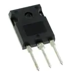
TO-247
• Tight parameters distribution
• Safe paralleling
• Low thermal resistance
TO-3P
• Low VF soft recovery co-packaged diode
• Lead free package
Figure 1. Internal schematic diagram
C (2 or TAB)
Applications
• Induction heating
• Microwave oven
• Resonant converters
Description
G (1)
This device is an IGBT developed using an
advanced proprietary trench gate field stop
structure. The device is part of the new HB series
of IGBTs, which represent an optimum
compromise between conduction and switching
losses to maximize the efficiency of any
frequency converter. Furthermore, a slightly
positive VCE(sat) temperature coefficient and very
tight parameter distribution result in safer
paralleling operation.
E (3)
Table 1. Device summary
Order code
Marking
Package
Packaging
STGW40H60DLFB
GW40H60DLFB
TO-247
Tube
STGWT40H60DLFB
GWT40H60DLFB
TO-3P
Tube
March 2014
This is information on a product in full production.
DocID024370 Rev 4
1/17
www.st.com
17
�Contents
STGW40H60DLFB, STGWT40H60DLFB
Contents
1
Electrical ratings . . . . . . . . . . . . . . . . . . . . . . . . . . . . . . . . . . . . . . . . . . . . 3
2
Electrical characteristics . . . . . . . . . . . . . . . . . . . . . . . . . . . . . . . . . . . . . 4
2.1
Electrical characteristics (curves) . . . . . . . . . . . . . . . . . . . . . . . . . . . . . . . . 6
3
Test circuits
4
Package mechanical data . . . . . . . . . . . . . . . . . . . . . . . . . . . . . . . . . . . . 12
5
2/17
. . . . . . . . . . . . . . . . . . . . . . . . . . . . . . . . . . . . . . . . . . . . . 11
4.1
TO-247, STGW40H60DLFB . . . . . . . . . . . . . . . . . . . . . . . . . . . . . . . . . . . 12
4.2
TO-3P, STGWT40H60DLFB . . . . . . . . . . . . . . . . . . . . . . . . . . . . . . . . . . 14
Revision history . . . . . . . . . . . . . . . . . . . . . . . . . . . . . . . . . . . . . . . . . . . 16
DocID024370 Rev 4
�STGW40H60DLFB, STGWT40H60DLFB
1
Electrical ratings
Electrical ratings
Table 2. Absolute maximum ratings
Symbol
Value
Unit
Collector-emitter voltage (VGE = 0)
600
V
IC
Continuous collector current at TC = 25 °C
80
A
IC
Continuous collector current at TC = 100 °C
40
A
ICP(1)
Pulsed collector current
160
A
VGE
Gate-emitter voltage
±20
V
IF
Continuous forward current at TC = 25 °C
80
A
IF
Continuous forward current at TC = 100 °C
40
A
IFP(1)
Pulsed forward current
160
A
PTOT
Total dissipation at TC = 25 °C
283
W
TSTG
Storage temperature range
- 55 to 150
°C
Operating junction temperature
- 55 to 175
°C
Value
Unit
VCES
TJ
Parameter
1. Pulse width limited by maximum junction temperature
Table 3. Thermal data
Symbol
Parameter
RthJC
Thermal resistance junction-case IGBT
0.53
°C/W
RthJC
Thermal resistance junction-case diode
1.47
°C/W
RthJA
Thermal resistance junction-ambient
50
°C/W
DocID024370 Rev 4
3/17
�Electrical characteristics
2
STGW40H60DLFB, STGWT40H60DLFB
Electrical characteristics
TJ = 25 °C unless otherwise specified.
Table 4. Static characteristics
Symbol
Parameter
Test conditions
Collector-emitter
V(BR)CES breakdown voltage
(VGE = 0)
IC = 2 mA
Min.
VF
IF = 40 A TJ = 125 °C
1.3
IF = 40 A TJ = 175 °C
1.25
VCE = VGE, IC = 1 mA
ICES
Collector cut-off current
(VGE = 0)
IGES
Gate-emitter leakage
current (VCE = 0)
V
1.8
1.55
Gate threshold voltage
2
1.7
IF = 40 A
VGE(th)
Unit
V
1.6
VGE = 15 V, IC = 40 A
Collector-emitter saturation
TJ = 125 °C
voltage
VGE = 15 V, IC = 40 A
TJ = 175 °C
Forward on-voltage
Max.
600
VGE = 15 V, IC = 40 A
VCE(sat)
Typ.
5
6
1.8
V
7
V
VCE = 600 V
25
µA
VGE = ± 20 V
250
nA
Table 5. Dynamic characteristics
Symbol
4/17
Parameter
Cies
Input capacitance
Coes
Output capacitance
Cres
Reverse transfer
capacitance
Qg
Total gate charge
Test conditions
VCE = 25 V, f = 1 MHz,
VGE = 0
VCC = 480 V, IC = 40 A,
VGE = 15 V, see Figure 27
Qge
Gate-emitter charge
Qgc
Gate-collector charge
DocID024370 Rev 4
Min.
Typ.
Max.
Unit
-
5412
-
pF
-
198
-
pF
-
107
-
pF
-
210
-
nC
-
39
-
nC
-
82
-
nC
�STGW40H60DLFB, STGWT40H60DLFB
Electrical characteristics
Table 6. IGBT switching characteristics (inductive load)
Symbol
td(off)
tf
Parameter
Test conditions
Turn-off delay time
Current fall time
Eoff(1)
Turn-off switching losses
td(off)
Turn-off delay time
tf
Eoff(1)
Current fall time
Turn-off switching losses
VCE = 400 V, IC = 40 A,
RG = 10 Ω, VGE = 15 V, see
Figure 25
VCE = 400 V, IC = 40 A,
RG = 10 Ω, VGE = 15 V,
TJ = 175 °C, see Figure 25
Min.
Typ.
Max.
142
Unit
ns
-
27.6
-
ns
-
363
-
µJ
141
ns
-
61
-
ns
-
764
-
µJ
Unit
1. Turn-off losses include also the tail of the collector current.
Table 7. IGBT switching characteristics (capacitive load)
Symbol
Eoff(1)
Parameter
Turn-off switching losses
Test conditions
Min.
Typ.
Max.
VCC = 320 V, RG = 10 Ω,
IC = 40 A, L = 100 µH,
Csnub = 20 nF, see Figure 26
-
190
-
VCC = 320 V, RG = 10 Ω,
IC = 40 A, L = 100 µH,
Csnub = 20 nF, TJ = 175 °C,
see Figure 26
µJ
-
290
-
1. Turn-off losses include also the tail of the collector current.
DocID024370 Rev 4
5/17
�Electrical characteristics
2.1
STGW40H60DLFB, STGWT40H60DLFB
Electrical characteristics (curves)
Figure 2. Power dissipation vs. case
temperature
GIPD011020131205FSR
Ptot
(W)
250
Figure 3. Collector current vs. case temperature
GIPD011020131155FSR
IC
(A)
80
70
200
60
50
150
40
100
30
20
VGE ≥ 15V, TJ ≤ 175 °C
50
10
0
0
25
50
Figure 4. Output characteristics (TJ = 25°C)
IC
(A)
140
0
0
75 100 125 150 175 TC(°C)
GIPD011020131123FSR
VGE=15V
11V
75 100 125 150 175 TC(°C)
Figure 5. Output characteristics (TJ = 175°C)
GIPD011020131135FSR
IC
(A)
140
120
120
100
100
80
50
25
VGE=15V
11V
9V
80
9V
60
60
40
40
20
20
7V
0
0
1
2
3
4
Figure 6. VCE(sat) vs. junction temperature
GIPD011020131319FSR
VCE(sat)
(V)
VGE= 15V
2.6
0
0
VCE(V)
IC= 80A
VCE(V)
GIPD011020131325FSR
2
TJ= 175°C
VGE= 15V
2.4
2.2
1.8
4
3
VCE(sat)
(V)
2.2
IC= 40A
2
Figure 7. VCE(sat) vs. collector current
2.4
2
1
TJ= 25°C
1.8
1.6
TJ= -40°C
1.6
IC= 20A
1.4
1.2
-50
6/17
1.4
1.2
0
50
100
150
TJ(°C)
1.0
DocID024370 Rev 4
0
20
40
60
80 IC(A)
�STGW40H60DLFB, STGWT40H60DLFB
Electrical characteristics
Figure 8. Collector current vs. switching
frequency
GIPD011020131340FSR
IC
(A)
Figure 9. Forward bias safe operating area
GIPD011020131351FSR
IC
(A)
100
TC= 80°C
100
80
TC= 100°C
10 μs
60
10
100 μs
40
Rectangular current shape
(duty cycle= 0.5, VCC= 400V, Rg=4.7Ω,
VGE = 0/15 V, TJ = 175 °C)
20
0
1
10
f(kHz)
Figure 10. Transfer characteristics
GIPD011020131146FSR
IC
(A)
0.1
10
1
100
VCE(V)
Figure 11. Diode VF vs. forward current
GIPD011020131402FSR
VF
(V)
TJ= -40°C
VCE=5V
140
-40°C
120
2.1
TJ= 25°C
100
80
1 ms
Single pulse
Tc= 25°C, TJ