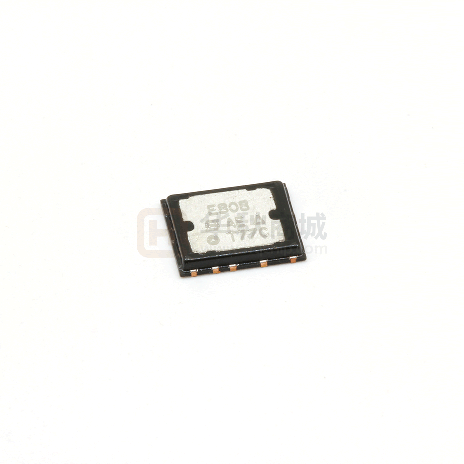
SiE808DF
Vishay Siliconix
N-Channel 20-V (D-S) MOSFET
FEATURES
PRODUCT SUMMARY
• Halogen-free According to IEC 61249-2-21
Definition
• TrenchFET® Gen II Power MOSFET
• Ultra Low Thermal Resistance Using TopExposed PolarPAK® Package for DoubleSided Cooling
• Leadframe-Based New Encapsulated Package
- Die Not Exposed
- Same Layout Regardless of Die Size
• Low Qgd/Qgs Ratio Helps Prevent Shoot-Through
• 100 % Rg and UIS Tested
• Compliant to RoHS directive 2002/95/EC
ID (A)a
RDS(on) (Ω)e
Silicon
Limit
0.0016 at VGS = 10 V
220
60
0.0025 at VGS = 4.5 V
117
60
VDS (V)
20
Package
Qg (Typ.)
Limit
46 nC
Package Drawing
www.vishay.com/doc?72945
PolarPAK
10
D
9
G
8
S
7
S
6
D
6
7
8
9
10
APPLICATIONS
D
D
S
G
• VRM
• DC/DC Conversion: Low-Side
• Synchronous Rectification
D
D
G
D
1
G
2
S
S
3
4
Top View
D
5
5
4
3
2
1
S
Bottom View
Top surface is connected to pins 1, 5, 6, and 10
N-Channel MOSFET
For Related Documents
Ordering Information: SiE808DF-T1-E3 (Lead (Pb)-free)
SiE808DF-T1-GE3 (Lead (Pb)-free and Halogen-free)
www.vishay.com/ppg?73739
ABSOLUTE MAXIMUM RATINGS TA = 25 °C, unless otherwise noted
Parameter
Drain-Source Voltage
Gate-Source Voltage
Symbol
VDS
VGS
TC = 25 °C
Continuous Drain Current (TJ = 150 °C)
TC = 70 °C
TA = 25 °C
TA = 70 °C
Pulsed Drain Current
ID
IDM
Continuous Source-Drain Diode Current
TC = 25 °C
TA = 25 °C
IS
Single Pulse Avalanche Current
Avalanche Energy
L = 0.1 mH
IAS
EAS
Limit
20
± 20
220 (Silicon Limit)
60a (Package Limit)
60a
45b, c
36b, c
100
60a
4.3b, c
35
61
125
80
5.2b, c
3.3b, c
- 55 to 150
260
Unit
V
A
mJ
TC = 25 °C
TC = 70 °C
PD
Maximum Power Dissipation
W
TA = 25 °C
TA = 70 °C
TJ, Tstg
Operating Junction and Storage Temperature Range
°C
Soldering Recommendations (Peak Temperature)d, e
Notes:
a. Package limited is 60 A.
b. Surface Mounted on 1" x 1" FR4 board.
c. t = 10 s.
d. See Solder Profile (www.vishay.com/doc?73257). The PolarPAK is a leadless package. The end of the lead terminal is exposed copper (not
plated) as a result of the singulation process in manufacturing. A solder fillet at the exposed copper tip cannot be guaranteed and is not
required to ensure adequate bottom side solder interconnection.
e. Rework Conditions: manual soldering with a soldering iron is not recommended for leadless components.
Document Number: 73739
S09-1337-Rev. B, 13-Jul-09
www.vishay.com
1
�SiE808DF
Vishay Siliconix
THERMAL RESISTANCE RATINGS
Parameter
t ≤ 10 s
Maximum Junction-to-Ambienta, b
Maximum Junction-to-Case (Drain Top)
Steady State
Maximum Junction-to-Case (Source)a, c
Notes:
a. Surface Mounted on 1" x 1" FR4 board.
b. Maximum under Steady State conditions is 68 °C/W.
c. Measured at source pin (on the side of the package).
Symbol
RthJA
RthJC (Drain)
RthJC (Source)
Typical
20
0.8
2.2
Maximum
24
1
2.7
Unit
°C/W
SPECIFICATIONS TJ = 25 °C, unless otherwise noted
Parameter
Symbol
Test Conditions
Min.
VDS
ΔVDS/TJ
ΔVGS(th)/TJ
VGS = 0 V, ID = 250 µA
20
Gate-Source Threshold Voltage
Gate-Source Leakage
VGS(th)
IGSS
Zero Gate Voltage Drain Current
IDSS
On-State Drain Currenta
ID(on)
VDS = VGS , ID = 250 µA
VDS = 0 V, VGS = ± 20 V
VDS = 20 V, VGS = 0 V
VDS = 20 V, VGS = 0 V, TJ = 55 °C
VDS ≥ 5 V, VGS = 10 V
VGS = 10 V, ID = 25 A
VGS = 4.5 V, ID = 25 A
VDS = 10 V, ID = 25 A
Typ.
Max.
Unit
Static
Drain-Source Breakdown Voltage
VDS Temperature Coefficient
VGS(th) Temperature Coefficient
Drain-Source On-State Resistancea
Forward Transconductancea
Dynamicb
Input Capacitance
Output Capacitance
Reverse Transfer Capacitance
Total Gate Charge
RDS(on)
gfs
Ciss
Coss
Crss
Qg
ID = 250 µA
VDS = 10 V, VGS = 0 V, f = 1 MHz
VDS = 10 V, VGS = 10 V, ID = 25 A
VDS = 10 V, VGS = 4.5 V, ID = 20 A
Qgs
Gate-Source Charge
Qgd
Gate-Drain Charge
Rg
f = 1 MHz
Gate Resistance
td(on)
Turn-On Delay Time
VDD = 10 V, RL = 1 Ω
tr
Rise Time
td(off)
ID ≅ 10 A, VGEN = 4.5 V, Rg = 1 Ω
Turn-Off Delay Time
tf
Fall Time
td(on)
Turn-On Delay Time
VDD = 10 V, RL = 1 Ω
tr
Rise Time
ID ≅ 10 A, VGEN = 10 V, Rg = 1 Ω
td(off)
Turn-Off Delay Time
tf
Fall Time
Drain-Source Body Diode Characteristics
TC = 25 °C
IS
Continuous Source-Drain Diode Current
ISM
Pulse Diode Forward Currenta
IS = 10 A
VSD
Body Diode Voltage
trr
Body Diode Reverse Recovery Time
Qrr
Body Diode Reverse Recovery Charge
IF = 10 A, dI/dt = 100 A/µs, TJ = 25 °C
ta
Reverse Recovery Fall Time
tb
Reverse Recovery Rise Time
Notes:
a. Pulse test; pulse width ≤ 300 µs, duty cycle ≤ 2 %.
b. Guaranteed by design, not subject to production testing.
1.5
V
26.5
- 7.3
2.3
mV/°C
3
± 100
1
10
25
V
nA
µA
A
0.0013
0.0021
95
8800
1600
600
102
46
26
8
0.9
180
215
50
15
25
55
55
10
0.8
56
60
26
30
0.0016
0.0025
Ω
S
pF
155
70
1.35
270
325
75
25
40
85
85
15
60
100
1.2
85
90
nC
Ω
ns
A
V
ns
nC
ns
Stresses beyond those listed under “Absolute Maximum Ratings” may cause permanent damage to the device. These are stress ratings only, and functional operation
of the device at these or any other conditions beyond those indicated in the operational sections of the specifications is not implied. Exposure to absolute maximum
rating conditions for extended periods may affect device reliability.
www.vishay.com
2
Document Number: 73739
S09-1337-Rev. B, 13-Jul-09
�SiE808DF
Vishay Siliconix
TYPICAL CHARACTERISTICS 25 °C, unless otherwise noted
20
100
VGS = 10 V thru 5 V
16
VGS = 4 V
I D - Drain Current (A)
I D - Drain Current (A)
80
60
40
12
8
TC = 125 °C
4
20
TC = 25 °C
VGS = 3 V
0
0.00
0.05
0.10
0.15
0.20
0.25
TC = - 55 °C
0
1.5
0.30
2.0
2.5
3.0
3.5
VDS - Drain-to-Source Voltage (V)
VGS - Gate-to-Source Voltage (V)
Output Characteristics
Transfer Characteristics
4.0
10 000
0.0030
8000
0.0026
C - Capacitance (pF)
RDS(on) - On-Resistance (Ω)
Ciss
VGS = 4.5 V
0.0022
0.0018
6000
4000
VGS = 10 V
0.0014
Coss
2000
Crss
0
0.0010
0
20
40
60
80
0
100
5
10
20
VDS - Drain-to-Source Voltage (V)
ID - Drain Current (A)
On-Resistance vs. Drain Current and Gate Voltage
Capacitance
1.6
10
VGS = 4.5 V, 10 V
ID = 25 A
ID = 20 A
1.4
VDS = 10 V
6
VDS = 16 V
4
(Normalized)
8
RDS(on) - On-Resistance
VGS - Gate-to-Source Voltage (V)
15
1.2
1.0
0.8
2
0
0
20
40
60
80
100
120
0.6
- 50
- 25
0
25
50
75
100
125
Qg - Total Gate Charge (nC)
TJ - Junction Temperature (°C)
Gate Charge
On-Resistance vs. Junction Temperature
Document Number: 73739
S09-1337-Rev. B, 13-Jul-09
150
www.vishay.com
3
�SiE808DF
Vishay Siliconix
TYPICAL CHARACTERISTICS 25 °C, unless otherwise noted
0.0050
RDS(on) - Drain-to-Source On-Resistance (Ω)
I S - Source Current (A)
100
TJ = 150 °C
10
TJ = 25 °C
ID = 25 A
0.0045
0.0040
0.0035
0.0030
0.0025
125 °C
0.0020
25 °C
0.0015
0.0010
1
0.00
0.2
0.4
0.6
0.8
2
1.0
4
6
8
10
VGS - Gate-to-Source Voltage (V)
VSD - Source-to-Drain Voltage (V)
On-Resistance vs. Gate-to-Source Voltage
Source-Drain Diode Forward Voltage
2.8
50
2.6
40
2.4
Power (W)
VGS(th) (V)
ID = 250 µA
2.2
2.0
1.8
30
20
1.6
10
1.4
1.2
- 50
- 25
0
25
50
75
100
125
0
0.01
150
0.1
1
10
100
1000
Time (s)
TJ - Temperature (°C)
Single Pulse Power, Junction-to-Ambient
Threshold Voltage
100
Limited by RDS(on)*
ID - Drain Current (A)
1 ms
10 ms
10
100 ms
1
1s
10 s
TA = 25 °C
Single Pulse
0.1
DC
BVDSS
Limited
0.01
0.01
0.1
1
10
100
VDS - Drain-to-Source Voltage (V)
* VDS > minimum VGS at which RDS(on) is specified
Safe Operating Area, Junction-to-Ambient
www.vishay.com
4
Document Number: 73739
S09-1337-Rev. B, 13-Jul-09
�SiE808DF
Vishay Siliconix
TYPICAL CHARACTERISTICS 25 °C, unless otherwise noted
140
300
120
Power Dissipation (W)
I D - Drain Current (A)
250
200
150
100
50
100
80
60
40
20
Package Limited
0
0
0
25
50
75
100
TC - Case Temperature (°C)
Current Derating*
125
150
25
50
75
100
125
150
TC - Case Temperature (°C)
Power Derating, Junction-to-Case
* The power dissipation PD is based on TJ(max) = 150 °C, using junction-to-case thermal resistance, and is more useful in settling the upper
dissipation limit for cases where additional heatsinking is used. It is used to determine the current rating, when this rating falls below the package
limit.
Document Number: 73739
S09-1337-Rev. B, 13-Jul-09
www.vishay.com
5
�SiE808DF
Vishay Siliconix
TYPICAL CHARACTERISTICS 25 °C, unless otherwise noted
Normalized Effective Transient
Thermal Impedance
2
1
Duty Cycle = 0.5
0.2
Notes:
0.1
PDM
0.1
0.05
t1
t2
1. Duty Cycle, D =
t1
t2
2. Per Unit Base = RthJA = 55 °C/W
0.02
3. TJM - TA = PDMZthJA(t)
Single Pulse
4. Surface Mounted
0.01
10-4
10-3
10-2
10-1
1
Square Wave Pulse Duration (s)
10
100
600
Normalized Thermal Transient Impedance, Junction-to-Ambient
Normalized Effective Transient
Thermal Impedance
2
1
Duty Cycle = 0.5
0.2
0.1
0.05
0.1
0.02
Single Pulse
0.01
10-4
10-3
10 -2
10 -1
1
Square Wave Pulse Duration (s)
Normalized Thermal Transient Impedance, Junction-to-Case (Drain Top)
Normalized Effective Transient
Thermal Impedance
2
1
Duty Cycle = 0.5
0.2
0.1
0.1
0.05
Single Pulse
0.01
10-4
0.02
10-3
10-2
10-1
1
Square Wave Pulse Duration (s)
Normalized Thermal Transient Impedance, Junction-to-Source
Vishay Siliconix maintains worldwide manufacturing capability. Products may be manufactured at one of several qualified locations. Reliability data for Silicon
Technology and Package Reliability represent a composite of all qualified locations. For related documents such as package/tape drawings, part marking, and
reliability data, see www.vishay.com/ppg?73739.
www.vishay.com
6
Document Number: 73739
S09-1337-Rev. B, 13-Jul-09
�Package Information
Vishay Siliconix
POLARPAK™ OPTION L
M4
Product datasheet/information page contain
links to applicable package drawing.
10
9
8
7
6
D
G
S
S
D
M2
M1
M3
D
G
S
1
2
3
S
4
c
D
5
A
(Top View)
b1 H4
H1
7
S
8
S
9
G
b1 H1
10
D
K4
6
D
θ
H3 b2 H2
b3
θ
P1
K3
Z
P1
T5
θ
T3
M3
View A
E
E1
T2
T4
T1
T3
θ
T5
M4
A
b4
K4
A1
K3
P1
b4
P1
K2
K1
D1
D
0.26
b5
S
4
b5
S
3
G
2
D
1
b5
View A
(Bottom View)
0.13
0.25
DETAIL Z
D
5
0.39
A
0.20
0.33
0.58
Document Number: 72945
Revision: 11-Aug-08
www.vishay.com
1
�Package Information
Vishay Siliconix
MILLIMETERS
INCHES
DIM
MIN.
NOM.
MAX.
MIN.
NOM.
MAX.
A
0.75
0.80
0.85
0.030
0.031
0.033
A1
0.00
-
0.05
0.000
-
0.002
b1
0.48
0.58
0.68
0.019
0.023
0.027
b2
0.41
0.51
0.61
0.016
0.020
0.024
b3
2.19
2.29
2.39
0.086
0.090
0.094
b4
0.89
1.04
1.19
0.035
0.041
0.047
b5
0.23
0.33
0.43
0.009
0.013
0.017
c
0.20
0.25
0.30
0.008
0.010
0.012
D
6.00
6.15
6.30
0.236
0.242
0.248
D1
5.74
5.89
6.04
0.226
0.232
0.238
E
5.01
5.16
5.31
0.197
0.203
0.209
E1
4.75
4.90
5.05
0.187
0.193
0.199
H1
0.23
-
-
0.009
-
-
H2
0.45
-
0.56
0.018
-
0.022
H3
0.31
0.41
0.51
0.012
0.016
0.020
H4
0.45
-
0.56
0.018
-
0.022
K1
4.22
4.37
4.52
0.166
0.172
0.178
K2
1.08
1.13
1.18
0.043
0.044
0.046
K3
1.37
-
-
0.054
-
-
K4
0.24
-
-
0.009
-
-
M1
4.30
4.50
4.70
0.169
0.177
0.185
M2
3.43
3.58
3.73
0.135
0.141
0.147
M3
0.22
-
-
0.009
-
-
M4
0.05
-
-
0.002
-
-
P1
0.15
0.20
0.25
0.006
0.008
0.010
T1
3.48
3.64
4.10
0.137
0.143
0.161
T2
0.56
0.76
0.95
0.022
0.030
0.037
T3
1.20
-
-
0.047
-
-
T4
3.90
-
-
0.153
-
-
T5
0
0.18
0.36
0.000
0.007
0.014
θ
0°
10°
12°
0°
10°
12°
ECN: T-08441-Rev. C, 11-Aug-08
DWG: 5946
Notes
Millimeters govern over inches.
www.vishay.com
2
Document Number: 72945
Revision: 11-Aug-08
�Application Note 826
Vishay Siliconix
RECOMMENDED MINIMUM PADS FOR PolarPAK® Option L and S
7.300
(0.287)
0.510
(0.020)
0.510
(0.020)
0.410
(0.016)
0.955
(0.038)
0.955
(0.038)
4.520
(0.178)
6.310
(0.248)
0.895
(0.035)
+
0.895
(0.035)
2.290
(0.090)
0.580
(0.023)
0.580
(0.023)
0.510
(0.020)
APPLICATION NOTE
Recommended Minimum for PolarPAK Option L and S
Dimensions in mm/(Inches)
No External Traces within Broken Lines
Dot indicates Gate Pin (Part Marking)
Return to Index
www.vishay.com
6
Document Number: 73491
Revision: 21-Jan-08
�Legal Disclaimer Notice
www.vishay.com
Vishay
Disclaimer
ALL PRODUCT, PRODUCT SPECIFICATIONS AND DATA ARE SUBJECT TO CHANGE WITHOUT NOTICE TO IMPROVE
RELIABILITY, FUNCTION OR DESIGN OR OTHERWISE.
Vishay Intertechnology, Inc., its affiliates, agents, and employees, and all persons acting on its or their behalf (collectively,
“Vishay”), disclaim any and all liability for any errors, inaccuracies or incompleteness contained in any datasheet or in any other
disclosure relating to any product.
Vishay makes no warranty, representation or guarantee regarding the suitability of the products for any particular purpose or
the continuing production of any product. To the maximum extent permitted by applicable law, Vishay disclaims (i) any and all
liability arising out of the application or use of any product, (ii) any and all liability, including without limitation special,
consequential or incidental damages, and (iii) any and all implied warranties, including warranties of fitness for particular
purpose, non-infringement and merchantability.
Statements regarding the suitability of products for certain types of applications are based on Vishay’s knowledge of
typical requirements that are often placed on Vishay products in generic applications. Such statements are not binding
statements about the suitability of products for a particular application. It is the customer’s responsibility to validate that a
particular product with the properties described in the product specification is suitable for use in a particular application.
Parameters provided in datasheets and / or specifications may vary in different applications and performance may vary over
time. All operating parameters, including typical parameters, must be validated for each customer application by the customer’s
technical experts. Product specifications do not expand or otherwise modify Vishay’s terms and conditions of purchase,
including but not limited to the warranty expressed therein.
Except as expressly indicated in writing, Vishay products are not designed for use in medical, life-saving, or life-sustaining
applications or for any other application in which the failure of the Vishay product could result in personal injury or death.
Customers using or selling Vishay products not expressly indicated for use in such applications do so at their own risk.
Please contact authorized Vishay personnel to obtain written terms and conditions regarding products designed for
such applications.
No license, express or implied, by estoppel or otherwise, to any intellectual property rights is granted by this document
or by any conduct of Vishay. Product names and markings noted herein may be trademarks of their respective owners.
© 2017 VISHAY INTERTECHNOLOGY, INC. ALL RIGHTS RESERVED
Revision: 08-Feb-17
1
Document Number: 91000
�