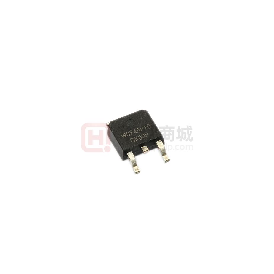
WSF45P10
P-Ch MOSFET
General Description
Product Summery
The WSF45P10 is the highest performance
trench P-Ch MOSFET with extreme high cell
density , which provide excellent RDSON and
gate charge for most of the small power
switching and load switch applications.
BVDSS
-100V
RDSON
ID
44mΩ
-40A
Applications
The WSF45P10 meet the RoHS and
Green Product requirement with full
function reliability approved.
z Inverters
TO-252 Pin Configuration
Features
z Advanced high cell density Trench technology
z Super Low Gate Charge
z Excellent Cdv/dt effect decline
z Green Device Available
Absolute Maximum Ratings
Symbol
Parameter
Rating
Unit
Common Ratings (TC=25°C Unless Otherwise Noted)
VDSS
Drain-Source Voltage
-100
VGSS
Gate-Source Voltage
±20
Maximum Junction Temperature
175
°C
-55 to 175
°C
-40
A
-120**
A
TJ
TSTG
IS
Storage Temperature Range
Diode Continuous Forward Current
TC=25°C
V
Mounted on Large Heat Sink
IDM
Pulsed Drain Current *
ID
Continuous Drain Current
PD
Maximum Power Dissipation
TC=25°C
-40
TC=100°C
-26
TC=25°C
136
TC=100°C
68
RθJC
Thermal Resistance-Junction to Case
1.1
RθJA
Thermal Resistance-Junction to Ambient
62.5
A
W
°C/W
Avalanche Ratings
EAS
Avalanche Energy, Single Pulsed
L=0.5mH
308***
mJ
Note: * Repetitive rating ; pulse width limiited by junction temperatur
** Drain current is limited by junction temperature
*** VD=-80V
www.winsok.tw
Page 1
Dec.2014
�WSF45P10
P-Ch MOSFET
Electrical Characteristics (TC=25°C Unless Otherwise Noted)
Symbol
Min.
Typ.
Max.
Unit
VGS=0V, IDS=-250µA
-100
-
-
V
VDS=-100 V, VGS=0V
-
-
-1
-
-
-10
-1
-2
-3
V
Parameter
Test Conditions
Static Characteristics
BVDSS
Drain-Source Breakdown Voltage
IDSS
Zero Gate Voltage Drain Current
VGS(th)
TJ=85°C
µA
Gate Threshold Voltage
VDS=VGS, IDS=-250µA
Gate Leakage Current
VGS=±20V, VDS=0V
-
-
±100
nA
RDS(ON)*
Drain-Source On-state Resistance
VGS=-10V, I DS=-20 A
-
44
55
mΩ
RDS(ON)*
Drain-Source On-state Resistance
VGS=-4.5V, I DS=-20A
-
47
58.5
mΩ
ISD=-20A, VGS=0V
-
-0.8
-1.2
V
-
70
-
ns
-
90
-
nC
-
2
-
Ω
-
5720
-
-
790
-
-
450
-
-
30
-
-
79
-
-
82
-
-
69
-
-
125
-
-
21
-
-
45
-
IGSS
Diode Characteristics
VSD *
Diode Forward Voltage
trr
Reverse Recovery Time
Qrr
Reverse Recovery Charge
ISD=-20A, dlSD/dt=-100A/µ s
Dynamic Characteristics
RG
Gate Resistance
Ciss
Input Capacitance
Coss
Output Capacitance
Crss
Reverse Transfer Capacitance
td(ON)
Turn-on Delay Time
Tr
Turn-on Rise Time
td(OFF)
Turn-off Delay Time
Tf
VGS=0V,VDS=0V,F=1MHz
VGS=0V,
VDS=-20V,
Frequency=1.0MHz
VDD=-50V, RG = 6 Ω,
IDS =-20A, VGS=-10V,
Turn-off Fall Time
pF
ns
Gate Charge Characteristics
Qg
Total Gate Charge
Qgs
Gate-Source Charge
Qgd
Gate-Drain Charge
VDS=-80V,VGS=-10V,
IDS=-20A
nC
Note * : Pulse test ; pulse width ≤300µs, duty cycle≤2%.
www.winsok.tw
Page 2
Dec.2014
�WSF45P10
P-Ch MOSFET
Typical Characteristics
Output Characteristics
Drain-Source On Resistance
60
80
VGS = -4.0,-4.5,-10V
-ID - Drain Current (A)
60
RDS(ON) - On - Resistance (mΩ)
70
-3.5V
50
40
-3V
30
20
-2V
10
0
50
VGS =-4.5V
45
VGS =-10V
40
35
0
1
2
3
4
5
0
6
10
20
30
40
-V DS - Drain-Source Voltage (V)
-I D - Drain Current (A)
Drain-Source On Resistance
Gate Threshold Voltage
1.6
120
100
80
60
50
40
30
0
2
4
6
8
10
1.2
1.0
0.8
0.6
0.4
0
25
50
75 100 125 150 175
Tj - Junction Temperature (°C)
-VGS - Gate - Source Voltage (V)
www.winsok.tw
1.4
0.2
-50 -25
12
50
IDS =-250µA
IDS=-20A
Normalized Threshold Vlotage
RDS(ON) - On - Resistance (mΩ)
55
Page 3
Dec.2014
�WSF45P10
P-Ch MOSFET
Typical Characteristics
Drain-Source On Resistance
Source-Drain Diode Forward
2.4
VGS =-10V
2.2
100
IDS =-20A
1.8
-IS - Source Current (A)
Normalized On Resistance
2.0
1.6
1.4
1.2
1.0
0.8
0.6
0.4
o
Tj=175 C
10
o
Tj=25 C
1
o
0.2
-50 -25
RON@Tj=25 C: 44m Ω
0
25
50
0.1
0.0
75 100 125 150 175
-0.6
-0.8
-1.0
-1.2
-VSD - Source-Drain Voltage (V)
Capacitance
Gate Charge
-1.4
10
Frequency=1MHz
10000
VDS= -80V
9
-VGS - Gate-source Voltage (V)
9000
C - Capacitance (pF)
-0.4
Tj - Junction Temperature (°C)
11000
8000
Ciss
7000
6000
5000
4000
3000
2000
1000
0
-0.2
Coss
Crss
0
5
10
15
20
25
30
35
-V DS - Drain - Source Voltage (V)
www.winsok.tw
7
6
5
4
3
2
1
0
40
IDS= -20A
8
0
20
40
60
80
100 120 140 160
QG - Gate Charge (nC)
Page 4
Dec.2014
�WSF45P10
P-Ch MOSFET
Typical Characteristics
Drain Current
Power Dissipation
140
-I D - Drain Current (A)
45
Ptot - Power (W)
120
100
80
60
40
40
35
30
25
20
15
10
20
5
o
0
TC=25 C
0
20 40
o
60
0
80 100 120 140 160 180 200
TC=25 C,VG=-10V
0
20
40
60 80 100 120 140 160 180 200
Tc - Case Temperature (°C)
Tc - Case Temperature (°C)
Safe Operation Area
ds
(
on
)L
im
it
100
100us
R
-ID - Drain Current (A)
1000
10
1ms
10ms
DC
1
o
TC=25 C
0.1
0.1
1
10
100
1000
-VDS - Drain - Source Voltage (V)
Thermal Transient Impedance
1
Normalized Effective Transient
Duty = 0.5
0.2
0.1
0.1
0.05
0.01
0.02
0.01
0.001
Single
Mounted on minimum pad
o
RθJA : 62.5 C/W
0.0001
0.0001
0.001
0.1
0.01
1
10
Square Wave Pulse Duration sec
www.winsok.tw
Page 5
Dec.2014
�WSF45P10
P-Ch MOSFET
Package Information
TO-252
E
A
E1
c2
L4
H
D
D1
L3
b3
c
b
e
SEE VIEW A
0
GAUGE PLANE
SEATING PLANE
0.25
A1
L
VIEW A
TO-252
S
Y
M
B
O
L
A
MIN.
MAX.
MIN.
MAX.
2.18
2.39
0.086
0.094
A1
-
0.13
-
0.005
b
0.50
0.89
0.020
0.035
0.215
RECOMMENDED LAND PATTERN
MILLIMETERS
INCHES
b3
4.95
5.46
0.195
c
0.46
0.61
0.018
0.024
c2
0.46
0.89
0.018
0.035
D
5.33
6.22
0.210
0.245
D1
4.57
6.00
0.180
E
6.35
6.73
0.250
0.236
0.265
E1
3.81
6.00
0.150
0.236
e
2.29 BSC
6.25 MIN.
6.8 MIN.
6.6
3 MIN.
0.090 BSC
H
9.40
10.41
0.370
0.410
L
0.90
1.78
0.035
0.070
L3
0.89
2.03
0.035
0.080
L4
-
1.02
-
0.040
0
0°
0°
8°
8°
2.286
1.5 MIN.
4.572
UNIT: mm
Note : Follow JEDEC TO-252 .
www.winsok.tw
Page 6
Dec.2014
�WSF45P10
P-Ch MOSFET
Classification Profile
www.winsok.tw
Page 7
Dec.2014
�WSF45P10
P-Ch MOSFET
Classification Reflow Profiles
Profile Feature
Sn-Pb Eutectic Assembly
Pb-Free Assembly
100 °C
150 °C
60-120 seconds
150 °C
200 °C
60-120 seconds
3 °C/second max.
3°C/second max.
183 °C
60-150 seconds
217 °C
60-150 seconds
See Classification Temp in table 1
See Classification Temp in table 2
Time (tP)** within 5°C of the specified
classification temperature (Tc)
20** seconds
30** seconds
Average ramp-down rate (Tp to Tsmax)
6 °C/second max.
6 °C/second max.
6 minutes max.
8 minutes max.
Preheat & Soak
Temperature min (Tsmin)
Temperature max (Tsmax)
Time (Tsmin to Tsmax) (ts)
Average ramp-up rate
(Tsmax to TP)
Liquidous temperature (TL)
Time at liquidous (tL)
Peak
(Tp)*
package
body
Temperature
Time 25°C to peak temperature
* Tolerance for peak profile Temperature (Tp) is defined as a supplier minimum and a user maximum.
** Tolerance for time at peak profile temperature (tp) is defined as a supplier minimum and a user maximum.
Table 1. SnPb Eutectic Process – Classification Temperatures (Tc)
3
Package
Volume mm
Thickness
很抱歉,暂时无法提供与“WSF45P10”相匹配的价格&库存,您可以联系我们找货
免费人工找货- 国内价格
- 1+2.65825
- 10+2.48675
- 50+2.22950
- 150+2.05800
- 300+1.93795
- 500+1.88650
- 国内价格
- 1+2.70600
- 100+2.09000
- 1250+1.81500
- 2500+1.72700
- 国内价格
- 1+3.34800
- 10+3.07800
- 30+2.90520
- 100+2.51640
- 500+2.27880