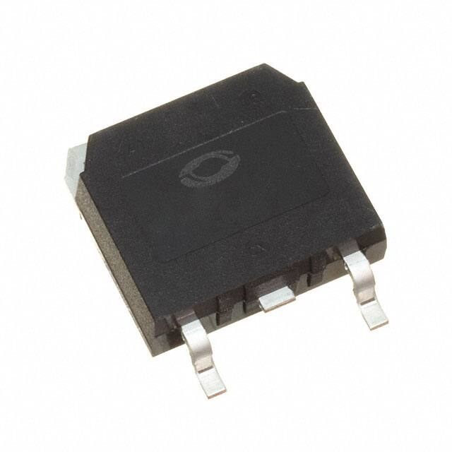
MSC080SMA120S Silicon Carbide N-Channel Power MOSFET
Product Overview
The silicon carbide (SiC) power MOSFET product line from Microsemi increases the performance over silicon
MOSFET and silicon IGBT solutions while lowering the total cost of ownership for high-voltage applications.
The MSC080SMA120S device is a 1200 V, 80 mΩ SiC MOSFET in a TO-268 (D3PAK) package.
Features
The following are key features of the MSC080SMA120S device:
• Low capacitances and low gate charge
• Fast switching speed due to low internal gate resistance (ESR)
• Stable operation at high junction temperature, TJ(max) = 175 °C
• Fast and reliable body diode
• Superior avalanche ruggedness
• RoHS compliant
Benefits
The following are benefits of the MSC080SMA120S device:
• High efficiency to enable lighter, more compact system
• Simple to drive and easy to parallel
• Improved thermal capabilities and lower switching losses
• Eliminates the need for external freewheeling diode
• Lower system cost of ownership
Applications
The MSC080SMA120S device is designed for the following applications:
• PV inverter, converter, and industrial motor drives
• Smart grid transmission and distribution
• Induction heating and welding
• H/EV powertrain and EV charger
• Power supply and distribution
050-7765 MSC080SMA120S Datasheet Revision A
1
�Device Specifications
Device Specifications
This section shows the specifications for the MSC080SMA120S device.
Absolute Maximum Ratings
The following table shows the absolute maximum ratings of the MSC080SMA120S device.
Table 1 • Absolute Maximum Ratings
Symbol
Parameter
Ratings
Unit
VDSS
Drain source voltage
1200
V
ID
Continuous drain current at TC = 25 °C
35
A
Continuous drain current at TC = 100 °C
25
IDM
Pulsed drain current 1
87
VGS
Gate-source voltage
23 to –10
V
PD
Total power dissipation at TC = 25 °C
182
W
Linear derating factor
1.21
W/°C
Note:
1. Repetitive rating: pulse width and case temperature limited by maximum junction temperature.
The following table shows the thermal and mechanical characteristics of the MSC080SMA120S device.
Table 2 • Thermal and Mechanical Characteristics
Symbol
Characteristic
Min
RθJC
Junction-to-case thermal resistance
TJ
Operating junction temperature
TSTG
Storage temperature
TL
Soldering temperature for 10 seconds (1.6 mm from case)
Wt
Package weight
050-7765 MSC080SMA120S Datasheet Revision A
Typ
Max
Unit
0.55
0.83
°C/W
–55
175
°C
–55
150
260
0.14
oz
4.0
g
2
�Device Specifications
Electrical Performance
The following table shows the static characteristics of the MSC080SMA120S device. TJ = 25 °C unless
otherwise specified.
Table 3 • Static Characteristics
Symbol
Characteristic
Test Conditions
Min
V(BR)DSS
Drain-source breakdown voltage
VGS = 0 V
1200
Typ
Max
Unit
V
ID = 100 µA
RDS(on)
Drain-source on resistance1
VGS = 20 V
80
100
mΩ
ID = 15 A
VGS(th)
Gate-source threshold voltage
VGS = VDS
1.8
2.8
V
–4.5
mV/°C
ID = 1 mA
ΔVGS(th)/
ΔTJ
Threshold voltage coefficient
IDSS
Zero gate voltage drain current
VGS = VDS
ID = 1 mA
VDS = 1200 V
100
µA
TJ = 25 °C
VGS = 0 V
VDS = 1200 V
500
TJ = 125 °C
VGS = 0 V
IGSS
Gate-source leakage current
VGS = 20 V
100
VGS = –10 V
100
nA
Note:
1. Pulse test: pulse width < 380 µs, duty cycle < 2%.
The following table shows the dynamic characteristics of the MSC080SMA120S device. TJ = 25 °C unless
otherwise specified.
Table 4 • Dynamic Characteristics
Symbol
Characteristic
Test Conditions
Ciss
Input capacitance
VGS = 0 V, VDD = 1000 V
Min
Typ
838
Max
Unit
pF
VAC = 25 mV, ƒ = 1 MHz
Crss
Reverse transfer capacitance
9
Coss
Output capacitance
84
Qg
Total gate charge
Qgs
Gate-source charge
VGS = –5 V/20 V, VDD = 800
64
nC
V ID = 15 A
050-7765 MSC080SMA120S Datasheet Revision A
12
3
�Device Specifications
Symbol
Characteristic
Qgd
Gate-drain charge
td(on)
Turn-on delay time
Test Conditions
Min
Typ
Max
Unit
19
VDD = 800 V, VGS = -5 V/20 V
5
ns
1
ID = 15 A, RG (ext) = 4 Ω
tr
Current rise time
Freewheeling diode =
4
MSC080SMA120S (VGS = –5 V)
td(off)
Turn-off delay time
21
tf
Current fall time
15
Eon
Turn-on switching energy 2
319
Eoff
Turn-off switching energy
52
td(on)
Turn-on delay time
VDD = 800 V, VGS = –5 V/20 V
4
µJ
ns
ID = 15 A, RG (ext) = 4 Ω1
tr
Current rise time
td(off)
Turn-off delay time
24
tf
Current fall time
19
Eon
Turn-on switching energy 2
199
Eoff
Turn-off switching energy
50
ESR
Equivalent series resistance
f = 1 MHz, 25 mV, drain short
1.9
Ω
SCWT
Short circuit withstand time
VDS = 960 V, VGS = 20 V
3
µS
1000
mJ
Freewheeling diode =
4
MSC015SDA120B
µJ
TC = 25 °C
EAS
Avalanche energy, single
pulse
VDS = 150 V, ID = 15 A
TC = 25 °C
Notes:
1. RG is total gate resistance excluding internal gate driver impedance.
2. Eon includes energy of the freewheeling diode.
050-7765 MSC080SMA120S Datasheet Revision A
4
�Device Specifications
The following table shows the body diode characteristics of the MSC080SMA120S device. TJ = 25 °C unless
otherwise specified.
Table 5 • Body Diode Characteristics
Symbol
Parameter
Test Conditions
Min
Typ
Max
Unit
VSD
Diode forward voltage
ISD = 15 A, VGS = 0 V
4.0
V
VSD
Diode forward voltage
ISD = 15 A, VGS = –5 V
4.2
V
trr
Reverse recovery time
ISD = 15 A, VGS = –5 V
34
ns
200
nC
6.5
A
VDD = 800 V
Qrr
Reverse recovery charge
IRRM
Reverse recovery current
dl/dt = –1000 A/µs
050-7765 MSC080SMA120S Datasheet Revision A
5
�Device Specifications
Typical Performance Curves
This section shows the typical performance curves of the MSC080SMA120S device.
Figure 1 • Drain Current vs. VDS
Figure 2 • Drain Current vs. VDS
Figure 3 • Drain Current vs. VDS
Figure 4 • Drain Current vs. VDS
050-7765 MSC080SMA120S Datasheet Revision A
6
�Device Specifications
Figure 5 • RDS(on) vs. Junction Temperature
Figure 7 • Capacitance vs. Drain-to-Source Voltage
Figure 9 • IDM vs. VDS 3rd Quadrant Conduction
Figure 6 • Gate Charge Characteristics
Figure 8 • IDM vs. Gate-to-Source Voltage
Figure 10 • IDM vs. VDS 3rd Quadrant Conduction
050-7765 MSC080SMA120S Datasheet Revision A
7
�Device Specifications
Figure 11 • VGS(th) vs. Junction Temp.
Figure 12 • Forward Safe Operating Area
Figure 13 • Maximum Transient Thermal Impedance
050-7765 MSC080SMA120S Datasheet Revision A
8
�Package Specification
Package Specification
This section shows the package specification of the MSC080SMA120S device.
Package Outline Drawing
The following figure illustrates the TO-268 package outline of the MSC080SMA120S device.
Figure 14 • Package Outline Drawing
The following table shows the TO-268 dimensions and should be used in conjunction with the package
outline drawing.
Table 6 • TO-268 Dimensions
Symbol
Min (mm)
Max (mm)
Min (in.)
Max (in.)
A
4.90
5.10
0.193
0.201
B
15.85
16.20
0.624
0.638
C
18.70
19.10
0.736
0.752
D
1.00
1.25
0.039
0.049
E
13.80
14.00
0.543
0.551
F
13.30
13.60
0.524
0.535
050-7765 MSC080SMA120S Datasheet Revision A
9
�Package Specification
Symbol
Min (mm)
Max (mm)
Min (in.)
Max (in.)
G
2.70
2.90
0.106
0.114
H
1.15
1.45
0.045
0.057
I
1.95
2.21
0.077
0.087
J
0.94
1.40
0.037
0.055
K
2.40
2.70
0.094
0.106
L
0.40
0.60
0.016
0.024
M
1.45
1.60
0.057
0.063
N
0.00
0.18
0.000
0.007
O
12.40
12.70
0.488
0.500
P
5.45 BSC (nom.)
Terminal 1
Gate
Terminal 2
Drain
Terminal 3
Source
Terminal 4
Drain
050-7765 MSC080SMA120S Datasheet Revision A
0.215 BSC (nom.)
10
�Legal
Microsemi
2355 W. Chandler Blvd.
Chandler, AZ 85224 USA
Within the USA: +1 (480) 792-7200
Fax: +1 (480) 792-7277
www.microsemi.com © 2020 Microsemi and
its corporate affiliates. All rights reserved.
Microsemi and the Microsemi logo are
trademarks of Microsemi Corporation and its
corporate affiliates. All other trademarks and
service marks are the property of their
respective owners.
Microsemi's product warranty is set forth in Microsemi's Sales Order Terms and Conditions. Information
contained in this publication is provided for the sole purpose of designing with and using Microsemi
products. Information regarding device applications and the like is provided only for your convenience
and may be superseded by updates. Buyer shall not rely on any data and performance specifications or
parameters provided by Microsemi. It is your responsibility to ensure that your application meets with
your specifications. THIS INFORMATION IS PROVIDED "AS IS." MICROSEMI MAKES NO REPRESENTATIONS
OR WARRANTIES OF ANY KIND WHETHER EXPRESS OR IMPLIED, WRITTEN OR ORAL, STATUTORY OR
OTHERWISE, RELATED TO THE INFORMATION, INCLUDING BUT NOT LIMITED TO ITS CONDITION, QUALITY,
PERFORMANCE, NON-INFRINGEMENT, MERCHANTABILITY OR FITNESS FOR A PARTICULAR PURPOSE.
IN NO EVENT WILL MICROSEMI BE LIABLE FOR ANY INDIRECT, SPECIAL, PUNITIVE, INCIDENTAL OR
CONSEQUENTIAL LOSS, DAMAGE, COST OR EXPENSE WHATSOEVER RELATED TO THIS INFORMATION
OR ITS USE, HOWEVER CAUSED, EVEN IF MICROSEMI HAS BEEN ADVISED OF THE POSSIBILITY OR THE
DAMAGES ARE FORESEEABLE. TO THE FULLEST EXTENT ALLOWED BY LAW, MICROSEMI’S TOTAL LIABILITY
ON ALL CLAIMS IN RELATED TO THIS INFORMATION OR ITS USE WILL NOT EXCEED THE AMOUNT OF
FEES, IF ANY, YOU PAID DIRECTLY TO MICROSEMI FOR THIS INFORMATION. Use of Microsemi devices
in life support, mission-critical equipment or applications, and/or safety applications is entirely at the
buyer’s risk, and the buyer agrees to defend and indemnify Microsemi from any and all damages, claims,
suits, or expenses resulting from such use. No licenses are conveyed, implicitly or otherwise, under any
Microsemi intellectual property rights unless otherwise stated.
Microsemi Corporation, a subsidiary of Microchip Technology Inc. (Nasdaq: MCHP),
and its corporate affiliates are leading providers of smart, connected and secure
embedded control solutions. Their easy-to-use development tools and
comprehensive product portfolio enable customers to create optimal designs which
reduce risk while lowering total system cost and time to market. These solutions
serve more than 120,000 customers across the industrial, automotive, consumer,
aerospace and defense, communications and computing markets. Headquartered
in Chandler, Arizona, the company offers outstanding technical support along with
dependable delivery and quality. Learn more at www.microsemi.com.
050-7765 | January 2020 | Released
050-7765 MSC080SMA120S Datasheet Revision A
11
�