LSIC1MO170T0750
Silicon Carbide MOSFET Datasheet
LSIC1MO170T0750
1700 V, 750 mOhm N-Channel SiC MOSFET
Product Summary
Characteristic
Value
VDS
1700
V
Typical RDS(ON)
750
mOhm
4.5
A
ID (TC
°C)
Unit
Features
• Optimized for high-frequency, high-efficiency
applications
• Extremely low gate charge and output
capacitance
• Low gate resistance for high-frequency switching
• Normally-off operations at all temperatures
• Ultra-low on-resistance
• Optimized package with separate driver source
pin
• MSL 1 Rated
Agency Approvals and Environmental
Environmental Approvals
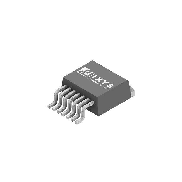
Pinout Diagram
Applications
• High-frequency applications
• Solar Inverters
• Switch Mode Power Supplies
• UPS
• Motor Drives
• High Voltage DC/DC Converters
• Battery Chargers
• Induction Heating
1
Specifications are subject to change without notice.
Read complete Disclaimer Notice at www.littelfuse.com/disclaimer-electronics.
© 2020 Littelfuse, Inc.
Revised: 9/4/2020
�LSIC1MO170T0750
Silicon Carbide MOSFET Datasheet
1. Maximum Ratings ...........................................................................................................................................3
2. Thermal Characteristics ..................................................................................................................................3
3. Electrical Characteristics .................................................................................................................................3
3.1. Static Characteristics (TJ = 25 °C unless otherwise specified) ................................................................3
3.2. Dynamic Characteristics (TJ = 25 °C unless otherwise specified) ...........................................................4
4. Reverse Diode Characteristics .......................................................................................................................4
5. Figure Data .....................................................................................................................................................5
6. Package Dimensions ......................................................................................................................................9
7. Part Numbering and Marking ..........................................................................................................................9
8. Packing Options ..............................................................................................................................................9
9. Packing Specifications ..................................................................................................................................10
2
Specifications are subject to change without notice.
Read complete Disclaimer Notice at www.littelfuse.com/disclaimer-electronics.
© 2020 Littelfuse, Inc.
Revised: 9/4/2020
�LSIC1MO170T0750
Silicon Carbide MOSFET Datasheet
1. Maximum Ratings
Characteristic
Symbol
Drain-Source Voltage
Conditions
Value
Unit
V
VDS
VGS = 0 V
1700
VGS = 20 V, TC = 25 °C
6.4
VGS = 20 V, TC = 100 °C
4.5
ID(pulse)
TC = 25 °C
11
A
PD
TC = 25 °C, TJ = 175 °C
65
W
Continuous Drain Current
ID
Pulsed Drain Current 1
Power Dissipation
VGS,MAX
Gate-Source Voltage
Absolute maximum values
Steady state
6 to +22
VGS,OP,TR 2
Transient, ttransient < 300 nsec
10 to +25
VGS,OP 3
Recommended DC operating values
5 to +20
Operating Junction Temperature
A
V
TJ
-
55 to +175
°C
Storage Temperature
TSTG
-
55 to +150
°C
Lead Temperature for Soldering (MSL 1
Rated)
TSOLD
-
260
°C
Footnote 1: Pulse width limited by TJ,MAX
Footnote 2: See Figure 21 for further information
Footnote 3: MOSFET can operate with VGS(OFF) = 0 V
dependent upon PCB layout. VGS(OFF) = 5 V provides added noise margin and faster turn-off speed
2. Thermal Characteristics
Characteristic
Symbol
Value
Unit
Maximum Thermal Resistance, junction-to-case
Rth,JC,MAX
2.3
°C/W
Maximum Thermal Resistance, junction-to-ambient
Rth,JA,MAX
40
°C/W
3. Electrical Characteristics
3.1. Static Characteristics (T
Characteristic
J
= 25 °C unless otherwise specified)
Symbol
Conditions
Drain-Source Breakdown Voltage
V(BR)DSS
Zero Gate Voltage Drain Current
IDSS
Gate Leakage Current
Drain-Source On-State Resistance
Gate Threshold Voltage
Gate Resistance
Value
Min
Typ
Max
VGS = 0 V, ID = 100 µA
1700
-
-
VDS = 1700, VGS = 0 V
-
0.05
10
VDS = 1700 V, VGS = 0 V, TJ = 175 °C
-
0.1
-
IGSS,F
VGS = 22 V, VDS = 0 V
-
-
100
IGSS,R
VGS = 6 V, VDS = 0 V
-
-
100
RDS(ON)
VGS(TH)
RG
ID = 2 A, VGS = 20 V
-
750
1000
ID = 2 A, VGS = 20 V, TJ = 175 °C
-
1550
-
VDS = VGS, ID = 1 mA
1.8
2.8
4.0
VDS = VGS, ID = 1 mA, TJ = 175 °C
-
1.9
-
Resonance method, Drain-Source
shorted1
-
29
-
Unit
V
µA
nA
V
Footnote 1: For a description of the resonance method for measuring RG, refer to the JEDEC Standard JESD24-11 test method
3
Specifications are subject to change without notice.
Read complete Disclaimer Notice at www.littelfuse.com/disclaimer-electronics.
© 2020 Littelfuse, Inc.
Revised: 9/4/2020
�LSIC1MO170T0750
Silicon Carbide MOSFET Datasheet
3.2. Dynamic Characteristics (T
J
Characteristic
= 25 °C unless otherwise specified)
Value
Symbol
Conditions
Turn-On Switching Energy
EON
Turn-Off Switching Energy
EOFF
VDD = 1200 V, ID = 2 A,
VGS = -5 / +20 V,
RG,ext
1.4 mH,
FWD = LSIC1MO170T0750
Min
Typ
Max
-
80
-
-
43
-
Total Per-Cycle Switching Energy
ETS
-
123
-
Input Capacitance
CISS
-
200
-
Output Capacitance
COSS
-
11.5
-
Reverse Transfer Capacitance
CRSS
-
1.7
-
COSS Stored Energy
EOSS
-
5.7
-
-
11
-
-
4
-
-
5
-
-
8
-
-
15
-
-
27
-
-
173
-
Total Gate Charge
Qg
Gate-Source Charge
Qgs
Gate-Drain Charge
Qgd
Turn-On Delay Time
td(on)
Rise Time
tr
Turn-Off Delay Time
td(off)
Fall Time
tf
VDD = 1000 V, VGS = 0 V,
f = 1 MHz, VAC = 25 mV
VDD = 1200 V, ID = 2 A,
VGS = -5 / +20 V
VDD = 1200 V, VGS = -5 / +20 V,
ID = 2 A, RG,ext
RL = 600
Timing relative to VDS
Unit
mJ
pF
µJ
nC
ns
4. Reverse Diode Characteristics
Characteristic
Symbol
Diode Forward Voltage
VSD
Continuous Diode Forward Current
Peak Diode Forward Current
1
IS
ISP
Value
Conditions
Min
Typ
Max
IS = 1 A, VGS = 0 V
-
3.6
-
IS = 1 A, VGS = 0 V, TJ = 175 °C
-
3.2
-
-
-
10
-
-
15
VGS = 0 V, TC = 25 °C
Unit
V
A
Footnote 1: Pulse width limited by TJ,MAX
4
Specifications are subject to change without notice.
Read complete Disclaimer Notice at www.littelfuse.com/disclaimer-electronics.
© 2020 Littelfuse, Inc.
Revised: 9/4/2020
�LSIC1MO170T0750
Silicon Carbide MOSFET Datasheet
5. Figure Data
Figure 2. Typical Transfer Characteristics
70
8
60
7
Drain Current, ID (A)
Power Dissipation, PD (W)
Figure 1. Maximum Power Dissipation (TJ = 175 °C)
50
40
30
20
TJ = 25 °C
6
5
4
175 °C
3
-55 °C
2
10
1
0
0
(VDS = 10 V)
-75
-25
25
75
125
175
0
5
Figure 3. Typical Output Characteristics (TJ = 25 °C)
20
9
8
8
VGS = 20 V
7
6
18 V
5
16 V
4
14 V
Drain Current, ID (A)
3
12 V
2
10 V
1
7
6
VGS = 20 V
5
18 V
16 V
4
14 V
12 V
3
10 V
2
1
0
0
0
2
4
6
8
10
0
2
Drain-Source Voltage, VDS (V)
4
6
8
10
Drain-Source Voltage, VDS (V)
Figure 5. Typical Output Characteristics (TJ = -55 °C)
Figure 6. Typical Reverse Conduction Characteristics (TJ = 25 °C)
9
Reverse Voltage, VSD (V)
8
7
6
5
4
3
2
1
0
0
7
VGS = 20 V
6
5
18 V
4
16 V
0.5
1
1.5
2
-5 V 0 V
3
5V
10 V 15 V
2.5
14 V
2
VGS = 20 V
12 V
1
3.5
10 V
4
0
0
2
4
6
8
3
10
Reverse Current, IS (A)
Drain Current, ID (A)
15
Figure 4. Typical Output Characteristics (TJ = 175 °C)
9
Drain Current, ID (A)
10
Gate-Source Voltage, VGS (V)
Case Temperature, TC (°C)
4.5
Drain-Source Voltage, VDS (V)
5
5
Specifications are subject to change without notice.
Read complete Disclaimer Notice at www.littelfuse.com/disclaimer-electronics.
© 2020 Littelfuse, Inc.
Revised: 9/4/2020
�LSIC1MO170T0750
Silicon Carbide MOSFET Datasheet
Figure 7. Typical Reverse Conduction Characteristics (TJ = 175 °C)
Figure 8. Typical Reverse Conduction Characteristics (TJ = -55 °C)
5
4
3
Reverse Voltage, VSD (V)
2
1
0
7
15 V
3.5
1.5
2
-5 V
5V
10 V 15 V
VGS = 20 V
3
3.5
4
4.5
4.5
5
5
Figure 10. Maximum Safe Operating Area (TC = 25 °C)
10
Duty = 0.5
0.3
Drain Current, ID (A)
Transient Thermal Impedance, Zth,JH
(Normalized to Rth,JC)
0V
2.5
1E+0
0.1
0.05
0.02
0.01
Pulse
10 µs
1
100 µs
1 ms
0.1
100 ms
Single Pulse
(Single Pulse)
1E-3
1E-06
0.01
1E-05
1E-04
1E-03
1E-02
1E-01
1E+00
0.1
1
Pulse Width (s)
10
100
1000
10000
Drain-Source Voltage, VDS (V)
Figure 11. Typical On-resistance vs. Drain Current
Figure 12. Normalized On-resistance vs. Junction Temperature
2.5
Normalized On-resistance, RDS(ON)
3500
On-resistance, RDS(ON) (mOhm)
0
1
Figure 9. Normalized Transient Thermal Impedance
1E-2
1
0.5
4
1E-1
2
1
3
5V
3
0
2.5
10 V
4
0.5
2
VGS = 20 V
5
0
1.5
-5 V 0 V
6
Reverse Current, IS (A)
6
Reverse Current, IS (A)
Reverse Voltage, VSD (V)
7
3000
2500
TJ = 175 °C
2000
-55 °C
1500
1000
25 °C
500
(VGS = 20 V)
0
2
1.5
1
0.5
(VGS = 20 V, ID = 2 A)
0
0
2
4
6
8
-75
Drain Current, ID (A)
-50
-25
0
25
50
75
100 125 150 175 200
Junction Temperature, TJ (°C)
6
Specifications are subject to change without notice.
Read complete Disclaimer Notice at www.littelfuse.com/disclaimer-electronics.
© 2020 Littelfuse, Inc.
Revised: 9/4/2020
�LSIC1MO170T0750
Silicon Carbide MOSFET Datasheet
Figure 13. Typical On-resistance vs. Junction Temperature
Figure 14. Typical Threshold Voltage
4.5
Threshold Voltage, VGS(TH) (V)
On-resistance, RDS(ON) (mOhm)
2
1.8
1.6
1.4
16 V
1.2
1
18 V
0.8
20 V
0.6
0.4
Conditions:
IDS = 2 A
VGS traces labeled
0.2
0
4
3.5
3
2.5
2
1.5
1
0.5
(ID = 1 mA, VDS = VGS)
0
-50
0
50
100
150
-75
-50
-25
Junction Temperature, TJ (°C)
0
25
50
75
100 125 150 175 200
Junction Temperature, TJ (°C)
Figure 15. Typical Junction Capacitances up to 1000 V
Figure 16. Typical Junction Capacitances up to 200 V
1000
1000
CISS
Capacitance (pF)
Capacitance (pF)
CISS
100
COSS
10
100
COSS
10
CRSS
CRSS
(f = 1 MHz)
1
0
200
(f = 1 MHz)
1
400
600
800
1000
0
50
Drain-Source Voltage, VDS (V)
Figure 17. Typical COSS Stored Energy EOSS
150
200
Figure 18. Typical Gate Charge
7
20
Gate-Source Voltage, VGS (V)
6
Stored Energy, EOSS (µJ)
100
Drain-Source Voltage, VDS (V)
5
4
3
2
1
15
10
5
0
(VDD = 1200 V, ID = 2 A)
0
-5
0
200
400
600
800
1000
0
Drain-Source Voltage, VDS (V)
2
4
6
8
10
12
Gate Charge, QG (nC)
7
Specifications are subject to change without notice.
Read complete Disclaimer Notice at www.littelfuse.com/disclaimer-electronics.
© 2020 Littelfuse, Inc.
Revised: 9/4/2020
�LSIC1MO170T0750
Silicon Carbide MOSFET Datasheet
Figure 20. Typical Switching Energy vs. External Gate Resistance
Figure 19. Typical Switching Energy vs. Drain Current
300
VDD = 1200 V
RG,ext = 2 Ohm
VGS = -5/+20 V
FWD = LSIC1MO170T0750
L = 1.4 mH
TJ = 25 °C
200
Switching Energy, ESW (µJ)
Switching Energy, ESW (µJ)
250
Etot
150
Eon
100
Eoff
50
VDD = 1200 V
ID = 2 A
VGS = -5/+20 V
FWD = LSIC1MO170T0750
L = 1.4 mH
TJ = 25 °C
250
200
Etot
150
Eon
100
Eoff
50
0
0
0
1
2
3
4
5
0
6
10
20
30
40
50
60
External Gate Resistance, RG,ext (Ohm)
Drain Current, ID (A)
Figure 21. VGS Waveform Definitions
+25 V
ttransient
+22 V
0V
ttransient
-6 V
-10 V
8
Specifications are subject to change without notice.
Read complete Disclaimer Notice at www.littelfuse.com/disclaimer-electronics.
© 2020 Littelfuse, Inc.
Revised: 9/4/2020
�LSIC1MO170T0750
Silicon Carbide MOSFET Datasheet
6. Package Dimensions
Millimeters
Symbol
Recommended Solder Pad Layout:
Min
Nom
Max
A
4.300
4.435
4.570
A1
0.000
0.125
0.250
b
0.500
0.600
0.700
c
0.330
0.490
0.650
C2
1.170
1.285
1.400
D
9.025
9.075
9.125
D1
4.656
4.733
4.810
E
10.130
10.180
10.230
E1
6.500
7.550
8.600
E2
6.778
7.223
7.665
e
1.220
1.270
1.320
H
15.043
16.178
17.121
L
2.324
2.512
2.700
Notes:
L1
1.160
1.418
1.676
1. Dimensions D & E do not include mold
flash. Mold flash shall not exceed 0.127
mm per side. These dimensions are
measured at the outermost extreme of the
plastic body.
L3
0.254
2. Package is designed for high voltage and
does not conform to JEDEC std.
3. Top package/marking surface finish: 16-18
VDI.
7. Part Numbering and Marking
SiC
= SiC
1
= Gen 1
MO
= MOSFET
170
= Voltage Rating (1700 V)
T
= TO-263-7L
0750
= RDS(ON) (750 mOhm)
YY
= Year
WW
= Week
D
= Special Code
ZZZZZZ-ZZ
= Lot Number
8. Packing Options
9
Part Number
Marking
LSIC1MO170T0750
SIC1MO170T0750
Packing
Mode
Tube
(50 Pcs)
M.O.Q.
400
Specifications are subject to change without notice.
Read complete Disclaimer Notice at www.littelfuse.com/disclaimer-electronics.
© 2020 Littelfuse, Inc.
Revised: 9/4/2020
�LSIC1MO170T0750
Silicon Carbide MOSFET Datasheet
9. Packing Specifications
For additional information please visit www.Littelfuse.com/powersemi
Disclaimer Notice - Littelfuse products are not designed for, and shall not be used for, any purpose (including, without limitation, automotive, military, aerospace, medical, lifesaving, life-sustaining or nuclear facility applications, devices intended for surgical implant into the body, or any other application in which the failure or lack of desired operation of
the product may result in personal injury, death, or property damage) other than those expressly forth in applicable Littelfuse product documentation. Littelfuse shall not be liable for
any claims or damages arising out of products used in applications not expressly intended by Littelfuse as set forth in applicable Littelfuse documentation.
Read complete Disclaimer Notice at www.littelfuse.com/disclaimer-electronics
10
Specifications are subject to change without notice.
Read complete Disclaimer Notice at www.littelfuse.com/disclaimer-electronics.
© 2020 Littelfuse, Inc.
Revised: 9/4/2020
�