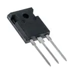
Power MOSFET
IXTX24N100
VDSS
ID25
RDS(on)
N-Channel Enhancement Mode
Avalanche Rated
=
=
≤
1000V
24A
Ω
400mΩ
PLUS247
Symbol
Test Conditions
VDSS
TJ = 25°C to 150°C
1000
V
VDGR
TJ = 25°C to 150°C, RGS = 1MΩ
1000
V
VGSS
Continuous
±20
V
VGSM
Transient
±30
V
ID25
TC = 25°C
24
A
IDM
TC = 25°C
96
A
IA
EAS
TC = 25°C
TC = 25°C
24
3
A
J
dV/dt
IS ≤ IDM, VDD ≤ VDSS, TJ ≤ 150°C
5
V/ns
PD
TC = 25°C
568
W
-55 ... +150
150
-55 ... +150
°C
°C
°C
300
260
°C
°C
20..120 / 4.5..27
N/lb.
6
g
TJ
TJM
Tstg
TL
TSOLD
1.6mm (0.062 in.) from Case for 10s
Plastic body for 10s
Md
Mounting Force
Maximum Ratings
Weight
Tab
G = Gate
S = Source
D = Drain
Tab = Drain
Features
•
•
•
•
•
International Standard Package
Low RDS (on) HDMOSTM Process
Rugged Polysilicon Gate Cell Structure
Avalanche Rated
Low Package Inductance
Advantages
• PLUS 247TM Package for Clip or Spring
Mounting
• Space Savings
• High Power Density
Applications
Symbol
Test Conditions
(TJ = 25°C, Unless Otherwise Specified)
Characteristic Values
Min. Typ. Max.
BVDSS
VGS = 0V, ID = 3mA
1000
VGS(th)
VDS = VGS, ID = 8mA
3.0
IGSS
VGS = ±20V, VDS = 0V
IDSS
VDS = VDSS, VGS = 0V
TJ = 125°C
RDS(on)
VGS = 10V, ID = 0.5 • ID25, Note 1
© 2010 IXYS CORPORATION, All rights reserved
V
5.5
V
±100 nA
• DC-DC Converters
• Battery Chargers
• Switch-Mode and Resonant-Mode
Power Supplies
• DC Choppers
• AC Motor Drives
• Temperature and Lighting Controls
50 μA
1 mA
400 mΩ
DS99201C(09/10)
�IXTX24N100
Symbol
Test Conditions
(TJ = 25°C, Unless Otherwise Specified)
gfs
Characteristic Values
Min.
Typ. Max.
VDS = 10V, ID = 0.5 • ID25, Note 1
15
Ciss
Coss
VGS = 0V, VDS = 25V, f = 1MHz
Crss
td(on)
tr
td(off)
tf
Resistive Switching Times
VGS = 10V, VDS = 0.5 • VDSS, ID = 0.5 • ID25
RG = 1Ω (External)
Qg(on)
Qgs
VGS = 10V, VDS = 0.5 • VDSS, ID = 0.5 • ID25
Qgd
PLUS 247TM (IXTX) Outline
27
S
8700
pF
785
pF
315
pF
35
ns
35
ns
75
ns
21
ns
267
nC
52
nC
142
nC
0.22 °C/W
RthJC
RthCS
0.15
°C/W
Source-Drain Diode
Symbol
Test Conditions
(TJ = 25°C, Unless Otherwise Specified)
Characteristic Values
Min. Typ.
Max.
IS
VGS = 0V
24
A
ISM
Repetitive, Pulse Width Limited by TJM
96
A
VSD
IF = 24A, VGS = 0V, Note 1
1.5
V
trr
IF = 24A, -di/dt = 100A/μs, VR = 100V, VGS = 0V
Note
850
Terminals:
Dim.
A
A1
A2
b
b1
b2
C
D
E
e
L
L1
Q
R
1 - Gate
2 - Drain
3 - Source
Millimeter
Min. Max.
4.83
5.21
2.29
2.54
1.91
2.16
1.14
1.40
1.91
2.13
2.92
3.12
0.61
0.80
20.80 21.34
15.75 16.13
5.45 BSC
19.81 20.32
3.81
4.32
5.59
6.20
4.32
4.83
Inches
Min. Max.
.190 .205
.090 .100
.075 .085
.045 .055
.075 .084
.115 .123
.024 .031
.819 .840
.620 .635
.215 BSC
.780 .800
.150 .170
.220 0.244
.170 .190
ns
1: Pulse test, t ≤ 300μs, duty cycle, d ≤ 2%.
IXYS reserves the right to change limits, test conditions, and dimensions.
IXYS MOSFETs and IGBTs are covered
4,835,592
by one or more of the following U.S. patents: 4,850,072
4,881,106
4,931,844
5,017,508
5,034,796
5,049,961
5,063,307
5,187,117
5,237,481
5,381,025
5,486,715
6,162,665
6,259,123 B1
6,306,728 B1
6,404,065 B1
6,534,343
6,583,505
6,683,344
6,727,585
7,005,734 B2
6,710,405 B2 6,759,692
7,063,975 B2
6,710,463
6,771,478 B2 7,071,537
7,157,338B2
�IXTX24N100
Fig. 1. Output Characteristics @ T J = 25ºC
Fig. 2. Extended Output Characteristics @ T J = 25ºC
55
24
VGS = 10V
7V
VGS = 10V
50
20
45
ID - Amperes
ID - Amperes
40
16
6V
12
7V
35
30
25
20
8
6V
15
10
4
5
5V
0
5V
0
0
1
2
3
4
5
6
7
8
9
0
5
10
15
25
30
Fig. 4. RDS(on) Normalized to ID = 12A Value vs.
Junction Temperature
Fig. 3. Output Characteristics @ T J = 125ºC
2.8
24
VGS = 10V
VGS = 10V
2.4
R DS(on) - Normalized
20
6V
ID - Amperes
20
VDS - Volts
VDS - Volts
16
12
8
5V
4
I D = 24A
2.0
I D = 12A
1.6
1.2
0.8
0
0.4
0
2
4
6
8
10
12
14
16
18
-50
20
-25
0
VDS - Volts
25
50
75
100
125
150
125
150
TJ - Degrees Centigrade
Fig. 5. RDS(on) Normalized to ID = 12A Value vs.
Drain Current
Fig. 6. Maximum Drain Current vs.
Case Temperature
28
2.6
VGS = 10V
2.4
24
TJ = 125ºC
20
2.0
ID - Amperes
R DS(on) - Normalized
2.2
1.8
1.6
1.4
TJ = 25ºC
16
12
8
1.2
4
1.0
0.8
0
0
5
10
15
20
25
30
35
ID - Amperes
© 2010 IXYS CORPORATION, All rights reserved
40
45
50
55
-50
-25
0
25
50
75
TC - Degrees Centigrade
100
�IXTX24N100
Fig. 8. Transconductance
Fig. 7. Input Admittance
60
45
TJ = - 40ºC
40
50
30
25
g f s - Siemens
ID - Amperes
35
TJ = 125ºC
20
25ºC
15
25ºC
40
125ºC
30
20
- 40ºC
10
10
5
0
0
3.0
3.5
4.0
4.5
5.0
5.5
6.0
6.5
7.0
0
5
10
15
20
VGS - Volts
30
35
40
45
50
Fig. 10. Gate Charge
Fig. 9. Forward Voltage Drop of Intrinsic Diode
70
10
VDS = 500V
9
60
I D = 12A
8
50
I G = 10mA
7
VGS - Volts
IS - Amperes
25
ID - Amperes
40
30
TJ = 125ºC
6
5
4
3
20
TJ = 25ºC
2
10
1
0
0
0.2
0.3
0.4
0.5
0.6
0.7
0.8
0.9
1.0
1.1
0
1.2
30
60
VSD - Volts
90
120
150
180
210
240
270
QG - NanoCoulombs
Fig. 12. Maximum Transient Thermal Impedance
Fig. 11. Capacitance
1.00
100,000
Ciss
10,000
Z(th)JC - ºC / W
Capacitance - PicoFarads
f = 1MHz
Coss
0.10
1,000
Crss
100
0
5
10
15
20
25
30
35
40
VDS - Volts
0.01
0.001
0.01
0.1
1
10
Pulse Width - Seconds
IXYS reserves the right to change limits, test conditions, and dimensions.
IXYS REF: F_24N100(9X)4-14-10
�Disclaimer Notice - Information furnished is believed to be accurate and reliable. However, users should independently
evaluate the suitability of and test each product selected for their own applications. Littelfuse products are not designed for,
and may not be used in, all applications. Read complete Disclaimer Notice at www.littelfuse.com/disclaimer-electronics.
�


 工商网监
湘ICP备2023018690号
工商网监
湘ICP备2023018690号
